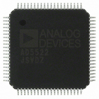
AD5522JSVDZ Analog Devices Inc, AD5522JSVDZ Datasheet - Page 6

AD5522JSVDZ
Manufacturer Part Number
AD5522JSVDZ
Description
IC, DAC, 16BIT, QFP-80
Manufacturer
Analog Devices Inc
Datasheet
1.AD5522JSVDZ.pdf
(64 pages)
Specifications of AD5522JSVDZ
Resolution (bits)
16bit
Input Channel Type
Serial
Supply Voltage Range - Digital
2.3V To 5.25V
Supply Current
36mA
Digital Ic Case Style
QFP
No. Of Pins
80
Data Interface
LVDS, Serial
Design Resources
Parametric Measurement Unit and Supporting Components for PAD Appls Using AD5522 and AD7685 (CN0104)
Lead Free Status / RoHS Status
Lead free / RoHS Compliant
Available stocks
Company
Part Number
Manufacturer
Quantity
Price
Company:
Part Number:
AD5522JSVDZ
Manufacturer:
WD
Quantity:
1 000
Company:
Part Number:
AD5522JSVDZ
Manufacturer:
Analog Devices Inc
Quantity:
10 000
Part Number:
AD5522JSVDZ
Manufacturer:
ADI/亚德诺
Quantity:
20 000
AD5522
SPECIFICATIONS
AVDD ≥ 10 V; AVSS ≤ −5 V; |AVDD − AVSS| ≥ 20 V and ≤ 33 V; DVCC = 2.3 V to 5.25 V; VREF = 5 V; REFGND = DUTGND = AGND = 0 V;
gain (M), offset (C), and DAC offset registers at default values; T
current, MV = measure voltage, MI = measure current, FS = full scale, FSR = full-scale range, FSVR = full-scale voltage range, FSCR =
full-scale current range.)
Table 1.
Parameter
FORCE VOLTAGE
MEASURE CURRENT
EXTFOHx Output Voltage Range
Differential Input Voltage Range
FOHx Output Voltage Range
Output Voltage Span
Offset Error
Offset Error Tempco
Gain Error
Gain Error Tempco
Linearity Error
Short-Circuit Current Limit
Noise Spectral Density (NSD)
Output Voltage Span
Offset Error
Offset Error Tempco
Gain Error
Gain Error Tempco
Linearity Error (MEASOUTx Gain = 1)
Linearity Error (MEASOUTx Gain = 0.2)
Common-Mode Voltage Range
Common-Mode Error (Gain = 5)
Common-Mode Error (Gain = 10)
Sense Resistors
2
2
2
2
2
2
2
2
2
2
Min
AVSS + 4
AVSS + 3
−50
−0.5
−0.01
−150
−10
−1.125
−0.5
−1
−0.5
−0.015
−0.01
−0.06
−0.11
−0.015
−0.06
−0.01
−0.01
AVSS + 4
−0.01
−0.005
Typ
22.5
−10
0.5
320
22.5
1
−2
200
50
5
0.5
1
Rev. D | Page 6 of 64
Max
AVDD − 4
AVDD − 3
+50
+0.5
+0.01
+150
+10
+1.125
+0.5
+1
+0.5
+0.015
+0.01
+0.06
+0.11
+0.015
+0.06
+0.01
+0.01
AVDD − 4
+0.01
+0.005
J
= 25°C to 90°C, unless otherwise noted. (FV = force voltage, FI = force
Unit
V
V
V
mV
μV/°C
% FSR
ppm/°C
% FSR
mA
mA
nV/√Hz
V
V
% FSCR
μV/°C
% FSCR
% FSCR
ppm/°C
% FSR
% FSR
% FSR
% FSR
% FSR
% FSR
% FSR
% FSR
V
% FSCR/V
% FSCR/V
kΩ
kΩ
kΩ
kΩ
MI gain = 10, AVDD = 28 V, AVSS = −5 V,
% of full-scale change at force output per V change
Sense resistors are trimmed to within 1%
Test Conditions/Comments
All current ranges from FOHx at full-scale current;
includes ±1 V dropped across sense resistor
External high current range at full-scale current;
does not include ±1 V dropped across sense resistor
Measured at midscale code; prior to calibration
Standard deviation = 20 μV/°C
Prior to calibration
Standard deviation = 0.5 ppm/°C
FSR = full-scale range (±10 V), gain and offset errors
calibrated out
±80 mA range
All other ranges
1 kHz, at FOHx in FV mode
Measure current = (I
amplifier gain = 5 or 10, unless otherwise noted
Voltage across R
Measure current block with VREF = 5 V, MEASOUT
scaling happens after
V(R
Referred to MI input; standard deviation = 4 μV/°C
Using internal current ranges
Measure current amplifier alone
Standard deviation = 2 ppm/°C
Measure current amplifier alone; internal sense resistor
25 ppm/°C
MI gain = 10
MI gain = 5
offset DAC = 0x0
MI gain = 10, AVDD = 10 V, AVSS = −23 V,
offset DAC = 0x0EDB7
MI gain = 10, AVDD = 15.25 V, AVSS = −15.25 V,
offset DAC = 0xA492
MI gain = 5, AVDD = 28 V, AVSS = −5 V,
offset DAC = 0x0
MI gain = 5, AVDD = 10 V, AVSS = −23 V,
offset DAC = 0xEDB7
MI gain = 5, AVDD = 15.25 V, AVSS = −15.25 V,
offset DAC = 0xA492
in DUT voltage
% of full-scale change at force output per V change
in DUT voltage
±5 μA range
±20 μA range
±200 μA range
±2 mA range
SENSE
) = ±1 V, measured with zero current flowing
SENSE
DUT
; gain = 5 or 10
× R
SENSE
× gain);


