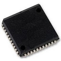
SC28L92A1A NXP Semiconductors, SC28L92A1A Datasheet - Page 13

SC28L92A1A
Manufacturer Part Number
SC28L92A1A
Description
UART, DUAL, 3.3V OR 5V, SMD, 28L92
Manufacturer
NXP Semiconductors
Datasheet
1.SC28L92A1B557.pdf
(73 pages)
Specifications of SC28L92A1A
No. Of Channels
2
Supply Voltage Range
2.97V To 3.63V, 4.5V To 5.5V
Operating Temperature Range
-40°C To +85°C
Digital Ic Case Style
PLCC
No. Of Pins
44
Svhc
No SVHC (18-Jun-2010)
Operating
RoHS Compliant
Data Rate
230.4Kilobaud
Uart Features
Programmable Channel Mode, Line Break Detection & Generation
Rohs Compliant
Yes
Available stocks
Company
Part Number
Manufacturer
Quantity
Price
Company:
Part Number:
SC28L92A1A
Manufacturer:
NXP
Quantity:
677
Company:
Part Number:
SC28L92A1A,512
Manufacturer:
NXP Semiconductors
Quantity:
10 000
Company:
Part Number:
SC28L92A1A,518
Manufacturer:
NXP Semiconductors
Quantity:
10 000
Company:
Part Number:
SC28L92A1A,529
Manufacturer:
NXP Semiconductors
Quantity:
10 000
Company:
Part Number:
SC28L92A1A529
Manufacturer:
NXP Semiconductors
Quantity:
135
NXP Semiconductors
Table 3.
[1]
6. Functional description
SC28L92_7
Product data sheet
Symbol
IP3
IP4
IP5
V
GND
n.c.
CC
HVQFN48 package die supply ground is connected to both GND pin and exposed center pad. GND pin must be connected to supply
ground for proper device operation. For enhanced thermal, electrical, and board level performance, the exposed pad needs to be
soldered to the board using a corresponding thermal pad on the board and for proper heat conduction through the board, thermal vias
need to be incorporated in the PCB in the thermal pad region.
Pin
PLCC44 QFP44 HVQFN48
3
43
42
44
22
1, 23, 34 23
Pin description for 68xxx bus interface (Motorola)
6.1.1 Data bus buffer
6.1.2 Operation control
6.1.3 Interrupt control
6.1 Block diagram
41
37
36
38, 39
16, 17
The SC28L92 DUART consists of the following eight major sections: data bus buffer,
operation control, interrupt control, timing, communications channels A and B, input port
and output port. Refer to
The data bus buffer provides the interface between the external and internal data buses. It
is controlled by the operation control block to allow read and write operations to take place
between the controlling CPU and the DUART.
The operation control logic receives operation commands from the CPU and generates
appropriate signals to internal sections to control device operation. It contains address
decoding and read and write circuits to permit communications with the microprocessor
via the data bus.
A single active LOW interrupt output (INTRN) is provided which is activated upon the
occurrence of any of eight internal events. Associated with the interrupt system are the
Interrupt Mask Register (IMR) and the Interrupt Status Register (ISR). The IMR can be
programmed to select only certain conditions to cause INTRN to be asserted. The ISR
can be read by the CPU to determine all currently active interrupting conditions. Outputs
OP3 to OP7 can be programmed to provide discrete interrupt outputs for the transmitter,
45
41
40
42
18
6, 13, 24,
25, 36, 37,
43
[1]
Type
I
I
I
Pwr
Pwr
-
Rev. 07 — 19 December 2007
3.3 V/5.0 V Dual Universal Asynchronous Receiver/Transmitter
Section 4 “Block
Description
Input 3: General purpose input or channel A transmitter external clock
input (TxCA). When the external clock is used by the transmitter, the
transmitted data is clocked on the falling edge of the clock.
Input 4: General purpose input or channel A receiver external clock
input (RxCA). When the external clock is used by the receiver, the
received data is sampled on the rising edge of the clock.
Input 5: General purpose input or channel B transmitter external clock
input (TxCB). When the external clock is used by the transmitter, the
transmitted data is clocked on the falling edge of the clock.
Power Supply: 3.3 V
Ground
Not connected
…continued
diagram”.
10 % or 5 V
10 % supply input.
SC28L92
© NXP B.V. 2007. All rights reserved.
13 of 73


