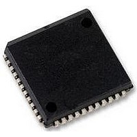
SC28L92A1A NXP Semiconductors, SC28L92A1A Datasheet - Page 26

SC28L92A1A
Manufacturer Part Number
SC28L92A1A
Description
UART, DUAL, 3.3V OR 5V, SMD, 28L92
Manufacturer
NXP Semiconductors
Datasheet
1.SC28L92A1B557.pdf
(73 pages)
Specifications of SC28L92A1A
No. Of Channels
2
Supply Voltage Range
2.97V To 3.63V, 4.5V To 5.5V
Operating Temperature Range
-40°C To +85°C
Digital Ic Case Style
PLCC
No. Of Pins
44
Svhc
No SVHC (18-Jun-2010)
Operating
RoHS Compliant
Data Rate
230.4Kilobaud
Uart Features
Programmable Channel Mode, Line Break Detection & Generation
Rohs Compliant
Yes
Available stocks
Company
Part Number
Manufacturer
Quantity
Price
Company:
Part Number:
SC28L92A1A
Manufacturer:
NXP
Quantity:
677
Company:
Part Number:
SC28L92A1A,512
Manufacturer:
NXP Semiconductors
Quantity:
10 000
Company:
Part Number:
SC28L92A1A,518
Manufacturer:
NXP Semiconductors
Quantity:
10 000
Company:
Part Number:
SC28L92A1A,529
Manufacturer:
NXP Semiconductors
Quantity:
10 000
Company:
Part Number:
SC28L92A1A529
Manufacturer:
NXP Semiconductors
Quantity:
135
NXP Semiconductors
Table 21.
Table 22.
OP1 and OP0 are the RTSN output and are controlled by the MR register
Table 23.
MR0 is accessed by setting the MR pointer to logic 0 via the command register command B.
SC28L92_7
Product data sheet
RxWATCHDOG
reset OP7
configure
OP7
7
7
7
ROPR - Reset Output Port bits Register (ROPR)
OPCR - Output Port Configuration Register
MR0A - Mode Register 0 channel A (address 0x0) bit allocation
7.3.1.1 Mode Register 0 channel A (MR0A)
7.3.1 Mode registers
reset OP6
configure
7.3 Register descriptions
OP6
RxINT[2]
6
6
Table 24.
6
Bit
7
6
5 and 4
reset OP5
configure
Symbol
RxWATCHDOG
RxINT[2]
TxINT[1:0]
OP5
MR0A - Mode Register 0 channel A (address 0x0) bit description
5
5
5
TxINT[1:0]
Rev. 07 — 19 December 2007
reset OP4
configure
3.3 V/5.0 V Dual Universal Asynchronous Receiver/Transmitter
OP4
4
4
Description
This bit controls the receiver watchdog timer.
When enabled, the watchdog timer will generate a receiver interrupt if
the receiver FIFO has not been accessed within 64 bit times of the
receiver 1 clock. The watchdog timer is used to alert the control
processor that data is in the Rx FIFO that has not been read. This
situation will occur when the byte count of the last part of a message
is not large enough to generate an interrupt.
The watchdog timer presents itself as a receiver interrupt with the
RxRDY bit set in SR and ISR.
Bit 2 of receiver FIFO interrupt level. This bit along with bit 6 of MR1
sets the fill level of the FIFO that generates the receiver interrupt.
Note that this control is split between MR0 and MR1. This is for
backward compatibility to the SC26C92 and SCC2681.
For the receiver these bits control the number of FIFO positions filled
when the receiver will attempt to interrupt. After the reset the receiver
FIFO is empty. The default setting of these bits cause the receiver to
attempt to interrupt when it has one or more bytes in it; see
Transmitter interrupt fill level. For the transmitter these bits control the
number of FIFO positions empty when the receiver will attempt to
interrupt; see
empty. It will then attempt to interrupt as soon as the transmitter is
enabled. The default setting (TxINT[1:0] = 00) condition the
transmitter to attempt to interrupt only when it is completely empty. As
soon as one byte is loaded, it is no longer empty and hence will
withdraw its interrupt request.
4
0 = disable
1 = enable
reset OP3
configure
FIFOSIZE
OP3
Table
3
3
3
26. After the reset the transmit FIFO has 8 bytes
EXTENDED II
BAUDRATE
reset OP2
configure
OP3
2
2
2
reset OP1
configure
TEST2
OP2
1
1
1
SC28L92
© NXP B.V. 2007. All rights reserved.
EXTENDED I
BAUDRATE
reset OP0
configure
OP2
Table
0
0
0
26 of 73
25.


