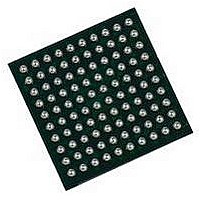
EP3C10M164C8N Altera, EP3C10M164C8N Datasheet - Page 150

EP3C10M164C8N
Manufacturer Part Number
EP3C10M164C8N
Description
IC CYCLONE III FPGA 402MHZ BGA-164
Manufacturer
Altera
Series
Cyclone IIIr
Specifications of EP3C10M164C8N
No. Of Logic Blocks
645
Family Type
Cyclone III
No. Of I/o's
106
I/o Supply Voltage
3.3V
Operating Frequency Max
402MHz
Operating Temperature Range
0°C To +85°C
Family Name
Cyclone III
Number Of Logic Blocks/elements
10320
# I/os (max)
106
Frequency (max)
402MHz
Process Technology
65nm
Operating Supply Voltage (typ)
1.2V
Logic Cells
10320
Ram Bits
423936
Operating Supply Voltage (min)
1.15V
Operating Supply Voltage (max)
1.25V
Operating Temp Range
0C to 85C
Operating Temperature Classification
Commercial
Mounting
Surface Mount
Pin Count
164
Package Type
MBGA
Lead Free Status / RoHS Status
Lead free / RoHS Compliant
Lead Free Status / RoHS Status
Lead free / RoHS Compliant
Available stocks
Company
Part Number
Manufacturer
Quantity
Price
- Current page: 150 of 350
- Download datasheet (8Mb)
8–6
Table 8–1. Cyclone III Device DQS and DQ Bus Mode Support for Each Side of the Device (Part 4 of 4)
Table 8–2. Cyclone III LS Device DQS and DQ Bus Mode Support for Each Side of the Device
Cyclone III Device Handbook, Volume 1
EP3C120
Notes to
(1) This device package does not support ×32 or ×36 mode.
(2) For the top side of the device, RUP, RDN, PLLCLKOUT3n, and PLLCLKOUT3p pins are shared with the DQ or DM pins to gain ×8 DQ group. You
(3) There is no DM pin support for these groups.
(4) The RUP and RDN pins are shared with the DQ pins. You cannot use these groups if you are using the RUP and RDN pins for OCT calibration.
(5) The ×8 DQ group can be formed in Bank 2.
(6) The ×8 DQ group can be formed in Bank 5.
(7) There is no DM and BWS# pins support for these groups.
(8) The RUP pin is shared with the DQ pin to gain ×9 or ×18 DQ group. You cannot use these groups if you are using the RUP and RDN pins for
EP3CLS70
Device
Device
cannot use these groups if you are using the RUP and RDN pins for on-chip termination (OCT) calibration or if you are using PLLCLKOUT3n
and PLLCLKOUT3p.
OCT calibration.
Table
8–1:
484-pin FineLine BGA
780-pin FineLine BGA
484-pin FineLine
BGA/
484-pin Ultra FineLine
BGA
780-pin FineLine BGA
(2)
Table 8–2
Cyclone III LS device only.
Package
Package
lists the numbers of DQS or DQ groups supported on each side of the
Left
Right
Top
Bottom
Left
Right
Top
Bottom
Bottom
Bottom
Right
Right
Side
Side
Left
Left
Top
Top
Number
Number
Groups
Groups
of ×8
Chapter 8: External Memory Interfaces in the Cyclone III Device Family
×8
4
4
4
4
4
4
6
6
2
2
2
2
4
4
6
6
Number
Number
Groups
Groups
of ×9
×9
2
2
2
2
2
2
2
2
2
2
2
2
2
2
2
2
Cyclone III Device Family Memory Interfaces Pin Support
Number
Number
Groups
Groups
of ×16
×16
2
2
2
2
2
2
2
2
1
1
1
1
2
2
2
2
© January 2010 Altera Corporation
Number
Number
Groups
Groups
of ×18
×18
(Note 1)
2
2
2
2
2
2
2
2
1
1
1
1
2
2
2
2
Number
Number
Groups
Groups
of ×32
(Part 1 of 2)
×32
—
—
—
—
1
1
1
1
1
1
1
1
1
1
1
1
Number
Number
Groups
Groups
of ×36
×36
—
—
—
—
1
1
1
1
1
1
1
1
1
1
1
1
Related parts for EP3C10M164C8N
Image
Part Number
Description
Manufacturer
Datasheet
Request
R

Part Number:
Description:
CYCLONE II STARTER KIT EP2C20N
Manufacturer:
Altera
Datasheet:

Part Number:
Description:
CPLD, EP610 Family, ECMOS Process, 300 Gates, 16 Macro Cells, 16 Reg., 16 User I/Os, 5V Supply, 35 Speed Grade, 24DIP
Manufacturer:
Altera Corporation
Datasheet:

Part Number:
Description:
CPLD, EP610 Family, ECMOS Process, 300 Gates, 16 Macro Cells, 16 Reg., 16 User I/Os, 5V Supply, 15 Speed Grade, 24DIP
Manufacturer:
Altera Corporation
Datasheet:

Part Number:
Description:
Manufacturer:
Altera Corporation
Datasheet:

Part Number:
Description:
CPLD, EP610 Family, ECMOS Process, 300 Gates, 16 Macro Cells, 16 Reg., 16 User I/Os, 5V Supply, 30 Speed Grade, 24DIP
Manufacturer:
Altera Corporation
Datasheet:

Part Number:
Description:
High-performance, low-power erasable programmable logic devices with 8 macrocells, 10ns
Manufacturer:
Altera Corporation
Datasheet:

Part Number:
Description:
High-performance, low-power erasable programmable logic devices with 8 macrocells, 7ns
Manufacturer:
Altera Corporation
Datasheet:

Part Number:
Description:
Classic EPLD
Manufacturer:
Altera Corporation
Datasheet:

Part Number:
Description:
High-performance, low-power erasable programmable logic devices with 8 macrocells, 10ns
Manufacturer:
Altera Corporation
Datasheet:

Part Number:
Description:
Manufacturer:
Altera Corporation
Datasheet:

Part Number:
Description:
Manufacturer:
Altera Corporation
Datasheet:

Part Number:
Description:
Manufacturer:
Altera Corporation
Datasheet:

Part Number:
Description:
CPLD, EP610 Family, ECMOS Process, 300 Gates, 16 Macro Cells, 16 Reg., 16 User I/Os, 5V Supply, 25 Speed Grade, 24DIP
Manufacturer:
Altera Corporation
Datasheet:


