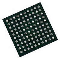
EP3C10M164C8N Altera, EP3C10M164C8N Datasheet - Page 251

EP3C10M164C8N
Manufacturer Part Number
EP3C10M164C8N
Description
IC CYCLONE III FPGA 402MHZ BGA-164
Manufacturer
Altera
Series
Cyclone IIIr
Specifications of EP3C10M164C8N
No. Of Logic Blocks
645
Family Type
Cyclone III
No. Of I/o's
106
I/o Supply Voltage
3.3V
Operating Frequency Max
402MHz
Operating Temperature Range
0°C To +85°C
Family Name
Cyclone III
Number Of Logic Blocks/elements
10320
# I/os (max)
106
Frequency (max)
402MHz
Process Technology
65nm
Operating Supply Voltage (typ)
1.2V
Logic Cells
10320
Ram Bits
423936
Operating Supply Voltage (min)
1.15V
Operating Supply Voltage (max)
1.25V
Operating Temp Range
0C to 85C
Operating Temperature Classification
Commercial
Mounting
Surface Mount
Pin Count
164
Package Type
MBGA
Lead Free Status / RoHS Status
Lead free / RoHS Compliant
Lead Free Status / RoHS Status
Lead free / RoHS Compliant
Available stocks
Company
Part Number
Manufacturer
Quantity
Price
- Current page: 251 of 350
- Download datasheet (8Mb)
Chapter 10: Hot-Socketing and Power-On Reset in the Cyclone III Device Family
Hot-Socketing Feature Implementation
Hot-Socketing Feature Implementation
Figure 10–1. Hot-socketing Circuit Block Diagram for Cyclone III Device Family
© December 2009
1
Altera Corporation
Each I/O pin has the circuitry shown in
not include CONF_DONE, nCEO, and nSTATUS pins to ensure that they are able to
operate during configuration. Thus, it is expected behavior for these pins to drive out
during power up and power down sequences.
Figure 10–1
family.
The POR circuit monitors the voltage level of power supplies and keeps the I/O pins
tristated until the device is in user mode. The weak pull-up resistor (R) in Cyclone III
device family I/O element (IOE) keeps the I/O pins from floating. The 3.0-V tolerance
control circuit permits the I/O pins to be driven by 3.0 V before V
supplies are powered up, and it prevents the I/O pins from driving out when the
device is not in user mode.
Altera uses GND as reference for hot-socketing operation and I/O buffer designs. To
ensure proper operation, Altera recommends connecting the GND between boards
before connecting the power supplies. This prevents the GND on your board from
being pulled up inadvertently by a path to power through other components on your
board. A pulled up GND can otherwise cause an out-of-specification I/O voltage or
current condition with the Altera
Resistor
Pull-Up
Weak
PAD
shows the hot-socketing circuit block diagram for Cyclone III device
R
V
CCIO
®
Input Buffer
to Logic Array
Tolerance
device.
Voltage
Control
Figure
Output Enable
10–1. The hot-socketing circuit does
Hot Socket
Pre-Driver
Output
Power On
Monitor
Reset
Cyclone III Device Handbook, Volume 1
CCIO
, V
CC
, and V
CCA
10–3
Related parts for EP3C10M164C8N
Image
Part Number
Description
Manufacturer
Datasheet
Request
R

Part Number:
Description:
CYCLONE II STARTER KIT EP2C20N
Manufacturer:
Altera
Datasheet:

Part Number:
Description:
CPLD, EP610 Family, ECMOS Process, 300 Gates, 16 Macro Cells, 16 Reg., 16 User I/Os, 5V Supply, 35 Speed Grade, 24DIP
Manufacturer:
Altera Corporation
Datasheet:

Part Number:
Description:
CPLD, EP610 Family, ECMOS Process, 300 Gates, 16 Macro Cells, 16 Reg., 16 User I/Os, 5V Supply, 15 Speed Grade, 24DIP
Manufacturer:
Altera Corporation
Datasheet:

Part Number:
Description:
Manufacturer:
Altera Corporation
Datasheet:

Part Number:
Description:
CPLD, EP610 Family, ECMOS Process, 300 Gates, 16 Macro Cells, 16 Reg., 16 User I/Os, 5V Supply, 30 Speed Grade, 24DIP
Manufacturer:
Altera Corporation
Datasheet:

Part Number:
Description:
High-performance, low-power erasable programmable logic devices with 8 macrocells, 10ns
Manufacturer:
Altera Corporation
Datasheet:

Part Number:
Description:
High-performance, low-power erasable programmable logic devices with 8 macrocells, 7ns
Manufacturer:
Altera Corporation
Datasheet:

Part Number:
Description:
Classic EPLD
Manufacturer:
Altera Corporation
Datasheet:

Part Number:
Description:
High-performance, low-power erasable programmable logic devices with 8 macrocells, 10ns
Manufacturer:
Altera Corporation
Datasheet:

Part Number:
Description:
Manufacturer:
Altera Corporation
Datasheet:

Part Number:
Description:
Manufacturer:
Altera Corporation
Datasheet:

Part Number:
Description:
Manufacturer:
Altera Corporation
Datasheet:

Part Number:
Description:
CPLD, EP610 Family, ECMOS Process, 300 Gates, 16 Macro Cells, 16 Reg., 16 User I/Os, 5V Supply, 25 Speed Grade, 24DIP
Manufacturer:
Altera Corporation
Datasheet:


