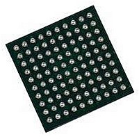
EP3C10M164C8N Altera, EP3C10M164C8N Datasheet - Page 343

EP3C10M164C8N
Manufacturer Part Number
EP3C10M164C8N
Description
IC CYCLONE III FPGA 402MHZ BGA-164
Manufacturer
Altera
Series
Cyclone IIIr
Specifications of EP3C10M164C8N
No. Of Logic Blocks
645
Family Type
Cyclone III
No. Of I/o's
106
I/o Supply Voltage
3.3V
Operating Frequency Max
402MHz
Operating Temperature Range
0°C To +85°C
Family Name
Cyclone III
Number Of Logic Blocks/elements
10320
# I/os (max)
106
Frequency (max)
402MHz
Process Technology
65nm
Operating Supply Voltage (typ)
1.2V
Logic Cells
10320
Ram Bits
423936
Operating Supply Voltage (min)
1.15V
Operating Supply Voltage (max)
1.25V
Operating Temp Range
0C to 85C
Operating Temperature Classification
Commercial
Mounting
Surface Mount
Pin Count
164
Package Type
MBGA
Lead Free Status / RoHS Status
Lead free / RoHS Compliant
Lead Free Status / RoHS Status
Lead free / RoHS Compliant
Available stocks
Company
Part Number
Manufacturer
Quantity
Price
- Current page: 343 of 350
- Download datasheet (8Mb)
Chapter 2: Cyclone III LS Device Data Sheet
I/O Timing
Table 2–38. Cyclone III LS Devices IOE Programmable Delay on Row Pins
I/O Timing
© December 2009
Input delay from the pin to the
internal cells
Input delay from the pin to the
input register
Delay from the output register to
the output pin
Input delay from the
dual-purpose clock pin to the
fan-out destinations
Notes to
(1) The incremental values for the settings are generally linear. For the exact values of each setting, use the latest version of the Quartus II software.
(2) The minimum and maximum offset timing numbers refer to the 0 setting available in the Quartus II software.
Table
Parameter
f
f
2–38:
Altera Corporation
DirectDrive technology and MultiTrack interconnect ensure predictable performance,
accurate simulation, and accurate timing analysis across all Cyclone III LS device
densities and speed grades.
Use the following methods to determine I/O timing:
■
■
Excel-based I/O timing provides pin timing performance for each device density and
speed grade. The data is typically used before designing the FPGA to get a timing
budget estimation as part of the link timing analysis. The Quartus II Timing Analyzer
provides a more accurate and precise I/O timing data based on the specifics of the
design after place-and-route is complete.
For more information about the Excel-based I/O timing spreadsheet, refer to the
Cyclone III Devices
All specifications are representative of worst-case supply voltage and junction
temperature conditions. Altera characterizes timing delays at the worst-case process,
minimum voltage, and maximum temperature for input register setup time (t
hold time (t
For more information about timing delay from the FPGA output to the receiving
device for system-timing analysis, refer to
for Altera Devices.
The Excel-based I/O timing
The Quartus II Timing Analyzer
Pad to I/O
dataout to core
Pad to I/O input
register
I/O output
register to pad
Pad to global
clock network
H
Paths Affected
).
Literature page on the Altera website.
Number
setting
12
of
7
8
2
Offset
Min
0
0
0
0
AN 366: Understanding I/O Output Timing
(Note
1.209 1.314 2.352 2.514 2.432
1.207 1.312 2.402 2.558 2.447
0.549 0.595 1.135 1.226 1.151
0.52
Fast Corner
I7
1),
(2)
0.54
C7
Cyclone III Device Handbook, Volume 2
Max Offset
1.052
C7
Slow Corner
1.16
C8
1.061
I7
SU
) and
Unit
ns
ns
ns
ns
2–25
Related parts for EP3C10M164C8N
Image
Part Number
Description
Manufacturer
Datasheet
Request
R

Part Number:
Description:
CYCLONE II STARTER KIT EP2C20N
Manufacturer:
Altera
Datasheet:

Part Number:
Description:
CPLD, EP610 Family, ECMOS Process, 300 Gates, 16 Macro Cells, 16 Reg., 16 User I/Os, 5V Supply, 35 Speed Grade, 24DIP
Manufacturer:
Altera Corporation
Datasheet:

Part Number:
Description:
CPLD, EP610 Family, ECMOS Process, 300 Gates, 16 Macro Cells, 16 Reg., 16 User I/Os, 5V Supply, 15 Speed Grade, 24DIP
Manufacturer:
Altera Corporation
Datasheet:

Part Number:
Description:
Manufacturer:
Altera Corporation
Datasheet:

Part Number:
Description:
CPLD, EP610 Family, ECMOS Process, 300 Gates, 16 Macro Cells, 16 Reg., 16 User I/Os, 5V Supply, 30 Speed Grade, 24DIP
Manufacturer:
Altera Corporation
Datasheet:

Part Number:
Description:
High-performance, low-power erasable programmable logic devices with 8 macrocells, 10ns
Manufacturer:
Altera Corporation
Datasheet:

Part Number:
Description:
High-performance, low-power erasable programmable logic devices with 8 macrocells, 7ns
Manufacturer:
Altera Corporation
Datasheet:

Part Number:
Description:
Classic EPLD
Manufacturer:
Altera Corporation
Datasheet:

Part Number:
Description:
High-performance, low-power erasable programmable logic devices with 8 macrocells, 10ns
Manufacturer:
Altera Corporation
Datasheet:

Part Number:
Description:
Manufacturer:
Altera Corporation
Datasheet:

Part Number:
Description:
Manufacturer:
Altera Corporation
Datasheet:

Part Number:
Description:
Manufacturer:
Altera Corporation
Datasheet:

Part Number:
Description:
CPLD, EP610 Family, ECMOS Process, 300 Gates, 16 Macro Cells, 16 Reg., 16 User I/Os, 5V Supply, 25 Speed Grade, 24DIP
Manufacturer:
Altera Corporation
Datasheet:


