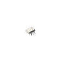
H11A5SR2VM Fairchild Semiconductor, H11A5SR2VM Datasheet - Page 6

H11A5SR2VM
Manufacturer Part Number
H11A5SR2VM
Description
Transistor Output Optocouplers Optocoupler Phototransistor
Manufacturer
Fairchild Semiconductor
Datasheet
1.H11A5SR2VM.pdf
(9 pages)
Specifications of H11A5SR2VM
Maximum Input Diode Current
60 mA
Maximum Reverse Diode Voltage
6 V
Output Device
Phototransistor
Output Type
DC
Configuration
1 Channel
Input Type
DC
Maximum Collector Emitter Voltage
30 V
Maximum Collector Emitter Saturation Voltage
0.4 V
Isolation Voltage
5300 Vrms
Maximum Forward Diode Voltage
1.5 V
Maximum Power Dissipation
250 mW
Maximum Operating Temperature
+ 100 C
Minimum Operating Temperature
- 55 C
Package / Case
PDIP-6 Gull Wing
Lead Free Status / RoHS Status
Lead free / RoHS Compliant
©2005 Fairchild Semiconductor Corporation
4NXXM, H11AXM Rev. 1.0.2
Package Dimensions
Through Hole
5.08 (Max.)
6.10–6.60
0.38 (Min.)
1.02–1.78
(0.86)
3.28–3.53
Pin 1
6
1
8.13–8.89
0.41–0.51
0.25–0.36
0.76–1.14
4
3
2.54–3.81
2.54 (Bsc)
(Max.)
5.08
8.43–9.90
3.28–3.53
Note:
All dimensions in mm.
Surface Mount
0.38 (Min.)
6.10–6.60
1.02–1.78
(0.86)
Pin 1
15° (Typ.)
7.62 (Typ.)
6
1
8.13–8.89
0.41–0.51
0.25–0.36
0.76–1.14
4
3
2.54 (Bsc)
0.20–0.30
6
5.08 (Max.)
0.4" Lead Spacing
6.10–6.60
0.38 (Min.)
(10.54)
1.02–1.78
(0.86)
3.28–3.53
Pin 1
0.16–0.88
(7.49)
Rcommended Pad Layout
(8.13)
(1.78)
6
1
8.13–8.89
0.41–0.51
0.25–0.36
0.76–1.14
(2.54)
(0.76)
0.20–0.30
4
3
2.54–3.81
2.54 (Bsc)
(1.52)
10.16–10.80
www.fairchildsemi.com
0.20–0.30


