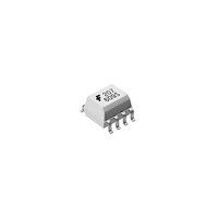
MOCD213R1VM Fairchild Semiconductor, MOCD213R1VM Datasheet

MOCD213R1VM
Specifications of MOCD213R1VM
Related parts for MOCD213R1VM
MOCD213R1VM Summary of contents
Page 1
... CATHODE 1 2 ANODE 2 3 CATHODE 2 4 ©2005 Fairchild Semiconductor Corporation MOCD213M Rev. 1.0.1 Description The MOCD213M device consists of two gallium arsenide infrared emitting diodes optically coupled to two mono- lithic silicon phototransistor detectors surface mountable, small outline plastic package ideally suited for high density applications and eliminates the need for through-the-board mounting ...
Page 2
... TOTAL DEVICE V Input-Output Isolation Voltage (f = 60Hz min.) ISO P Total Device Power Dissipation @ T D Derate above 25°C T Ambient Operating Temperature Range A T Storage Temperature Range stg ©2005 Fairchild Semiconductor Corporation MOCD213M Rev. 1.0 25°C Unless otherwise specified) A Rating = 25° 25° 25° Value ...
Page 3
... For this test, Pins and 4 are common and Pins and 8 are common rating of 2500 V for min. is equivalent to a rating of 3,000 V ISO AC(rms) 4. Current Transfer Ratio (CTR ©2005 Fairchild Semiconductor Corporation MOCD213M Rev. 1.0 25°C unless otherwise specified) A Test Conditions I = 30mA ...
Page 4
... I - LED FORWARD CURRENT (mA) F Fig. 3 Output Current vs. Ambient Temperature NORMALIZED 0.1 -80 -60 -40 - – AMBIENT TEMPERATURE ( A ©2005 Fairchild Semiconductor Corporation MOCD213M Rev. 1.0 0.1 100 0.01 1.6 1.4 1.2 1.0 0.8 0.6 0.4 0.2 0 100 120 o C) Fig. 5 Dark Current vs. Ambient Temperature ...
Page 5
... TEST CIRCUIT INPUT ©2005 Fairchild Semiconductor Corporation MOCD213M Rev. 1.0.1 = 10V R L 10% OUTPUT 90% Adjust I to produce I = 2mA F C Figure 6. Switching Time Test Circuit and Waveform 5 WAVEFORMS INPUT PULSE OUTPUT PULSE off www.fairchildsemi.com ...
Page 6
... Package drawings are provided as a service to customers considering Fairchild components. Drawings may change in any manner without notice. Please note the revision and/or date on the drawing and contact a Fairchild Semiconductor representative to verify or obtain the most recent revision. Package specifications do not expand the terms of Fairchild’s worldwide terms and conditions, specifi ...
Page 7
... Ordering Information Option Order Entry Identifi R2V Marking Information Definitions ©2005 Fairchild Semiconductor Corporation MOCD213M Rev. 1.0.1 V VDE 0884 R2 Tape and reel (2500 units per reel) R2V VDE 0884, Tape and reel (2500 units per reel) 1 D213 Fairchild logo Device number VDE mark (Note: Only appears on parts ordered with VDE option – ...
Page 8
... Carrier Tape Specifications 3.50 0.20 0.30 MAX 8.3 0.10 0.1 MAX User Direction of Feed Dimensions in mm ©2005 Fairchild Semiconductor Corporation MOCD213M Rev. 1.0.1 8.0 0.10 2.0 0.05 4.0 0.10 6.40 0.20 8 Ø1.5 MIN 1.75 0.10 5.5 0.05 12.0 0.3 5.20 0.20 Ø ...
Page 9
... Liquidous Temperature (T Time (t ) Maintained Above (T L Peak Body Package Temperature Time (t ) within 5°C of 260°C P Ramp-down Rate (T Time 25°C to Peak Temperature ©2005 Fairchild Semiconductor Corporation MOCD213M Rev. 1.0.1 Max. Ramp-up Rate = 3°C/S Max. Ramp-down Rate = 6°C/S Tsmax Preheat Area Tsmin t s 120 240 Time 25° ...
Page 10
... TRADEMARKS The following includes registered and unregistered trademarks and service marks, owned by Fairchild Semiconductor and/or its global subsidiaries, and is not intended exhaustive list of all such trademarks. Auto-SPM™ F-PFS™ FRFET Build it Now™ CorePLUS™ Global Power Resource CorePOWER™ ...


