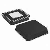
ADUC7061BCPZ32-RL Analog Devices Inc, ADUC7061BCPZ32-RL Datasheet - Page 34

ADUC7061BCPZ32-RL
Manufacturer Part Number
ADUC7061BCPZ32-RL
Description
DUAL 24-BIT AFE AND ARM 7 I.C
Manufacturer
Analog Devices Inc
Series
MicroConverter® ADuC7xxxr
Datasheet
1.EVAL-ADUC7061MKZ.pdf
(108 pages)
Specifications of ADUC7061BCPZ32-RL
Design Resources
USB Based Temperature Monitor Using ADuC7061 and an External RTD (CN0075) 4 mA-to-20 mA Loop-Powered Temperature Monitor Using ADuC7060/1 (CN0145)
Core Processor
ARM7
Core Size
16/32-Bit
Speed
10MHz
Connectivity
I²C, SPI, UART/USART
Peripherals
POR, PWM, Temp Sensor, WDT
Number Of I /o
8
Program Memory Size
32KB (32K x 8)
Program Memory Type
FLASH
Ram Size
4K x 8
Voltage - Supply (vcc/vdd)
2.375 V ~ 2.625 V
Data Converters
A/D 5x24b, 8x24b, D/A 1x14b
Oscillator Type
Internal
Operating Temperature
-40°C ~ 125°C
Package / Case
32-LFCSP
Lead Free Status / RoHS Status
Lead free / RoHS Compliant
Eeprom Size
-
Lead Free Status / RoHS Status
Lead free / RoHS Compliant
ADuC7060/ADuC7061
By writing to POWCON1, it is possible to further reduce power
consumption in active mode by powering down the UART, PWM
or I
0x76 in the instruction immediately before accessing POWCON1
and POWKEY4 must be set to 0xB1 in the instruction immediately
after.
For example, the following code enables the SPI/I
powers down the PWM and UART blocks.
POWKEY3 =0x76;
POWCON2 =0x4;
Uart; 0x4 SPI/I2C
POWKEY4 =0xB1;
Table 31. POWCON0 MMR Bit Designations
Bit
7
6
5
4
3
2:0
2
C/SPI blocks. To access POWCON1, POWKEY3 must be set to
Name
Reserved
XPD
PLLPD
PPD
COREPD
CD[2:0]
Description
This bit must always be set to 0.
XTAL power-down.
Cleared by user to power down the external crystal circuitry.
Set by user to enable the external crystal circuitry.
PLL power-down. Timer peripherals power down if driven from the PLL output clock. Timers driven from an active clock
source remain in normal power mode.
This bit is cleared to 0 to power down the PLL. The PLL cannot be powered down if either the core or peripherals are
enabled; Bit 3, Bit 4, and Bit 5 must be cleared simultaneously.
Set by default, and set by hardware on a wake-up event.
Peripherals power-down. The peripherals that are powered down by this bit are as follows:
SRAM, Flash/EE memory and GPIO interfaces, and SPI/I
Cleared to power down the peripherals. The peripherals cannot be powered down if the core is enabled; Bit 3 and Bit 4
must be cleared simultaneously.
Set by default and/or by hardware on a wake-up event. Wake-up timer (Timer1) can remain active.
Core power-down. If user code powers down the MCU, include a dummy MCU cycle after the power-down command is
written to POWCON0.
Cleared to power down the ARM core.
Set by default and set by hardware on a wake-up event.
Core clock depends on CD setting:
[000] = 10.24 MHz
[001] = 5.12 MHz
[010] = 2.56 MHz
[011] = 1.28 MHz [default value]
[100] = 640 kHz
[101] = 320 kHz
[110] = 160 kHz
[111] = 80 kHz
//0x100 PWM; 0x20
2
C blocks but,
Rev. B | Page 34 of 108
Power and Clock Control Registers
Name:
Address:
Default value:
Access:
Function:
Name:
Address:
Default value:
Access:
Function:
2
C and UART serial ports.
POWKEY1
0xXXXX
Write
0x01 must be written to this register in the
instruction immediately before writing to
POWCON0.
0xFFFF0404
When writing to POWCON0, the value of
POWCON0
0xFFFF0408
0x7B
Read and write
This register controls the clock divide bits
controlling the CPU clock (HCLK).


