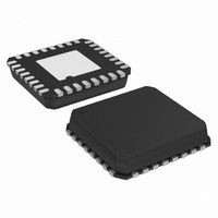
ADUC7061BCPZ32-RL Analog Devices Inc, ADUC7061BCPZ32-RL Datasheet - Page 35

ADUC7061BCPZ32-RL
Manufacturer Part Number
ADUC7061BCPZ32-RL
Description
DUAL 24-BIT AFE AND ARM 7 I.C
Manufacturer
Analog Devices Inc
Series
MicroConverter® ADuC7xxxr
Datasheet
1.EVAL-ADUC7061MKZ.pdf
(108 pages)
Specifications of ADUC7061BCPZ32-RL
Design Resources
USB Based Temperature Monitor Using ADuC7061 and an External RTD (CN0075) 4 mA-to-20 mA Loop-Powered Temperature Monitor Using ADuC7060/1 (CN0145)
Core Processor
ARM7
Core Size
16/32-Bit
Speed
10MHz
Connectivity
I²C, SPI, UART/USART
Peripherals
POR, PWM, Temp Sensor, WDT
Number Of I /o
8
Program Memory Size
32KB (32K x 8)
Program Memory Type
FLASH
Ram Size
4K x 8
Voltage - Supply (vcc/vdd)
2.375 V ~ 2.625 V
Data Converters
A/D 5x24b, 8x24b, D/A 1x14b
Oscillator Type
Internal
Operating Temperature
-40°C ~ 125°C
Package / Case
32-LFCSP
Lead Free Status / RoHS Status
Lead free / RoHS Compliant
Eeprom Size
-
Lead Free Status / RoHS Status
Lead free / RoHS Compliant
Name:
Address:
Default value:
Access:
Function:
Name:
Address:
Default value:
Access:
Function:
Table 32. POWCON1 MMR Bit Designations
Bit
15:9
8
7:6
5
4:3
2
1:0
Name:
Address:
Default value:
Access:
Function:
Name
Reserved
PWMOFF
Reserved
UARTOFF
Reserved
I2CSPIOFF
Reserved
POWKEY1
0xFFFF0404
0xXXXX
When writing to POWCON0, the value of
0x01 must be written to this register in the
instruction immediately before writing to
POWCON0.
POWKEY2
0xFFFF040C
0xXXXX
When writing to POWCON0, the value of
0xF4 must be written to this register in the
instruction immediately after writing to
POWCON0.
POWKEY4
0xFFFF043C
0xXXXX
When writing to POWCON1, the value of 0xB1 must be written to this register in the instruction immediately after
writing to POWCON1.
Write
Write
Write
Description
This bit must always be set to 0.
PWM power-down bit.
Set by user to 1 to enable the PWM block. This bit is set by default.
Cleared by user to 0 to power down the PWM block.
Reserved bits. Always clear these bits to 0.
UART power-down bit.
Set by user to 1 to enable the UART block. This bit is set by default.
Cleared by user to 0 to power down the UART block.
Reserved bits. Always clear these bits to 0.
I2C/SPI power-down bit.
Set by user to 1 to enable the I2C/SPI blocks. This bit is set by default.
Cleared by user to 0 to power down the I2C/SPI blocks.
Reserved Bits. Always clear these bits to 0.
Rev. B | Page 35 of 108
Name:
Address:
Default value:
Access:
Function:
Name:
Address:
Default value:
Access:
Function:
POWKEY3
0xFFFF0434
0xXXXX
Write
When writing to POWCON1, the value of
0x76 must be written to this register in the
instruction immediately after writing to
POWCON1.
POWCON1
0xFFFF0438
0x124
Read and write
This register controls the clock signal to the
PWM, UART and I2C/SPI blocks.
By disabling the clock to these blocks, power
consumption is reduced.
ADuC7060/ADuC7061


