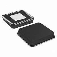
ADUC7061BCPZ32-RL Analog Devices Inc, ADUC7061BCPZ32-RL Datasheet - Page 46

ADUC7061BCPZ32-RL
Manufacturer Part Number
ADUC7061BCPZ32-RL
Description
DUAL 24-BIT AFE AND ARM 7 I.C
Manufacturer
Analog Devices Inc
Series
MicroConverter® ADuC7xxxr
Datasheet
1.EVAL-ADUC7061MKZ.pdf
(108 pages)
Specifications of ADUC7061BCPZ32-RL
Design Resources
USB Based Temperature Monitor Using ADuC7061 and an External RTD (CN0075) 4 mA-to-20 mA Loop-Powered Temperature Monitor Using ADuC7060/1 (CN0145)
Core Processor
ARM7
Core Size
16/32-Bit
Speed
10MHz
Connectivity
I²C, SPI, UART/USART
Peripherals
POR, PWM, Temp Sensor, WDT
Number Of I /o
8
Program Memory Size
32KB (32K x 8)
Program Memory Type
FLASH
Ram Size
4K x 8
Voltage - Supply (vcc/vdd)
2.375 V ~ 2.625 V
Data Converters
A/D 5x24b, 8x24b, D/A 1x14b
Oscillator Type
Internal
Operating Temperature
-40°C ~ 125°C
Package / Case
32-LFCSP
Lead Free Status / RoHS Status
Lead free / RoHS Compliant
Eeprom Size
-
Lead Free Status / RoHS Status
Lead free / RoHS Compliant
ADuC7060/ADuC7061
Bit
6:4
3:
1:0
ADC Filter Register
Name:
Address:
Default value:
Access:
Function:
Table 45. ADCFLT MMR Bit Designations
Bit
15
14
13:8
Name
CHOPEN
RAVG2
AF[5:0]
Name
ADC1REF[2:0]
BUF_BYPASS[1:0]
Description
Chop enable. Set by user to enable system chopping of all active ADCs. When this bit is set, the ADC has very low offset
errors and drift, but the ADC output rate is reduced by a factor of 3 if AF = 0 (see sinc3 decimation factor, Bits[6:0] in this
table). If AF > 0, then the ADC output update rate is the same with chop on or off. When chop is enabled, the settling time
is two output periods.
Running average-by-2 enable bit.
Set by user to enable a running-average-by-2 function, reducing ADC noise. This function is automatically enabled when
chopping is active. It is an optional feature when chopping is inactive, and if enabled (when chopping is inactive), does
not reduce the ADC output rate but does increase the settling time by one conversion period.
Cleared by user to disable the running average function.
Averaging factor (AF). The values written to these bits are used to implement a programmable first-order sinc3 post filter.
The averaging factor can further reduce ADC noise at the expense of output rate as described in Bits[6:0] (sinc3
decimation factor) in this table.
ADCFLT
0xFFFF0514
0x0007
Read and write
The ADC filter MMR is a 16-bit register that controls the speed and resolution of both the on-chip ADCs. Note that, if
ADCFLT is modified, the primary and auxiliary ADCs are reset.
Description
Auxiliary channel ADC reference select.
[000] = internal reference selected. In ADC low power mode, the voltage reference selection is controlled by
ADCMODE[5].
[001] = external reference inputs (VREF+, VREF−) selected. Set the HIGHEXTREF1 bit if reference voltage
exceeds 1.3 V.
[010] = auxiliary external reference inputs (ADC4/EXT_REF2IN+, ADC5/EXT_REF2IN−) selected. Set the
HIGHEXTREF1 bit if reference voltage exceeds 1.35 V.
[011] = (AVDD, AGND) divide-by-2 selected. If this configuration is selected, the HIGHEXTREF1 bit is set
automatically.
[100] = (AVDD, ADC3). ADC3 can be used as the negative input terminal for the reference source.
[101] to [111] = reserved.
Buffer bypass.
[00] = full buffer on. Both positive and negative buffer inputs active.
[01] = negative buffer is bypassed, positive buffer is on.
[10] = negative buffer is on, positive buffer is bypassed.
[11] = full buffer bypass. Both positive and negative buffer inputs are off.
Digital gain. Select for auxiliary ADC inputs.
[00] = ADC1 gain = 1.
[01] = ADC1 gain = 2.
[10] = ADC1 gain = 4.
[11] = ADC1 gain = 8.
Rev. B | Page 46 of 108


