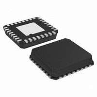
ADUC7061BCPZ32-RL Analog Devices Inc, ADUC7061BCPZ32-RL Datasheet - Page 85

ADUC7061BCPZ32-RL
Manufacturer Part Number
ADUC7061BCPZ32-RL
Description
DUAL 24-BIT AFE AND ARM 7 I.C
Manufacturer
Analog Devices Inc
Series
MicroConverter® ADuC7xxxr
Datasheet
1.EVAL-ADUC7061MKZ.pdf
(108 pages)
Specifications of ADUC7061BCPZ32-RL
Design Resources
USB Based Temperature Monitor Using ADuC7061 and an External RTD (CN0075) 4 mA-to-20 mA Loop-Powered Temperature Monitor Using ADuC7060/1 (CN0145)
Core Processor
ARM7
Core Size
16/32-Bit
Speed
10MHz
Connectivity
I²C, SPI, UART/USART
Peripherals
POR, PWM, Temp Sensor, WDT
Number Of I /o
8
Program Memory Size
32KB (32K x 8)
Program Memory Type
FLASH
Ram Size
4K x 8
Voltage - Supply (vcc/vdd)
2.375 V ~ 2.625 V
Data Converters
A/D 5x24b, 8x24b, D/A 1x14b
Oscillator Type
Internal
Operating Temperature
-40°C ~ 125°C
Package / Case
32-LFCSP
Lead Free Status / RoHS Status
Lead free / RoHS Compliant
Eeprom Size
-
Lead Free Status / RoHS Status
Lead free / RoHS Compliant
I
Each ADuC706x incorporates an I
configured as a fully I
as a fully I
data transfer, SDA and SCL, are configured in a wire-AND’ e d
format that allows arbitration in a multimaster system. These
pins require external pull-up resistors. Typical pull-up resistor
values are between 4.7 kΩ and 10 kΩ.
Users program the I
system). This ID can be modified any time that a transfer is not
in progress. The user can configure the interface to respond to
four slave addresses.
The transfer sequence of an I
device initiating a transfer by generating a start condition while
the bus is idle. The master transmits the slave device address
and the direction of the data transfer (read or write ) during the
initial address transfer. If the master does not lose arbitration
and the slave acknowledges, the data transfer is initiated. This
continues until the master issues a stop condition and the bus
becomes idle.
The I
at any given time. The same I
support master and slave modes.
The I
features:
•
•
GP0CON0 = BIT4 + BIT12;
GP0KEY1 = 0x7;
GP0CON1 = BIT1;
GP0KEY2 = 0x13;
2
C
Support for repeated start conditions. In master mode, the
ADuC706x can be programmed to generate a repeated
start. In slave mode, the ADuC706x recognizes repeated
start conditions.
In master and slave modes, the part recognizes both 7-bit
and 10-bit bus addresses.
2
2
C peripheral can be configured only as a master or a slave
C interface on the ADuC706x includes the following
2
C bus-compatible slave device. The two pins used for
2
C bus peripheral (addressed in the I
2
C-compatible I
2
2
C system consists of a master
C channel cannot simultaneously
2
C peripheral that can be
2
C bus master device or
// Select SPI/I
// Write to GP0KEY1
// Select I
// Write to GP0KEY2
2
C functionality for P0.1 and P0.3
2
C bus
2
Rev. B | Page 85 of 108
C alternative function for P0.1 and P0.3
•
•
•
•
•
•
CONFIGURING EXTERNAL PINS FOR I
FUNCTIONALITY
The I
pins of the ADuC706x device are P0.1 and P0.3. The function of
P0.1 is the I
I
Bit 4 and Bit 12 of the GP0CON0 register must be set to 1. Bit 1
of the GP0CON1 register must also be set to 1 to enable I
mode.
Note that, to write to GP0CON1, the GP0KEY1 register must
be set to 0x7 immediately before writing to GP0CON1. Also,
the GP0KEY2 register must be set to 0x13 immediately after
writing to GP0CON1. The following code example shows this
in detail:
2
C data signal (SDA). To configure P0.1 and P0.3 for I
In I
reads from a single slave up to 512 bytes in a single transfer
sequence.
Clock stretching is supported in both master and slave
modes.
In slave mode, the ADuC706x can be programmed to
return a no acknowledge (NACK). This allows the
validation of checksum bytes at the end of I
Bus arbitration in master mode is supported.
Internal and external loopback modes are supported for
I
The transmit and receive circuits in both master and slave
modes contain 2-byte FIFOs. Status bits are available to the
user to control these FIFOs.
2
2
C functions of the P0.1/SCLK/SCL and P0.3/MOSI/SDA
C hardware testing.
2
C master mode, the ADuC706x supports continuous
2
C clock signal (SCL) and the function of P0.3 is the
ADuC7060/ADuC7061
2
C
2
C transfers.
2
C mode,
2
C


