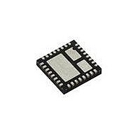
SIC417CD-T1-E3 Vishay, SIC417CD-T1-E3 Datasheet - Page 15

SIC417CD-T1-E3
Manufacturer Part Number
SIC417CD-T1-E3
Description
IC DRIVER MOSF SYNC BUCK 55MLPQ
Manufacturer
Vishay
Series
microBUCK™r
Datasheet
1.SIC417CD-T1-E3.pdf
(20 pages)
Specifications of SIC417CD-T1-E3
Topology
Step-Down (Buck) Synchronous (1), Linear (LDO) (1)
Function
Any Function
Number Of Outputs
2
Frequency - Switching
200kHz ~ 1MHz
Voltage/current - Output 1
0.5 V ~ 5.5 V, 10A
Voltage/current - Output 2
0.75 V ~ 5.25 V, 150mA
W/led Driver
No
W/supervisor
No
W/sequencer
No
Voltage - Supply
3 V ~ 28 V
Operating Temperature
-25°C ~ 125°C
Mounting Type
*
Package / Case
*
Output Voltage
0.5 V to 5.5 V
Output Current
10 A
Input Voltage
3 V to 28 V
Switching Frequency
200 KHz to 1 MHz
Mounting Style
SMD/SMT
Duty Cycle (max)
95 %
Primary Input Voltage
28V
No. Of Outputs
1
Voltage Regulator Case Style
MLPQ
No. Of Pins
32
Operating Temperature Range
-25°C To +125°C
Svhc
No SVHC
Rohs Compliant
Yes
Lead Free Status / RoHS Status
Lead free / RoHS Compliant
Lead Free Status / RoHS Status
Lead free / RoHS Compliant, Lead free / RoHS Compliant
Available stocks
Company
Part Number
Manufacturer
Quantity
Price
Part Number:
SIC417CD-T1-E3
Manufacturer:
VISHAY/威世
Quantity:
20 000
across C
the ESR of a standard capacitor. This ramp is then
capacitive-coupled into the FB pin via capacitor C
Dropout Performance
The output voltage adjusts range for continuous-conduction
operation is limited by the fixed 250 ns (typical) minimum
off-time of the one-shot. When working with low input
voltages, the duty-factor limit must be calculated using
worst-case values for on and off times. The duty-factor
limitation is shown by the next equation.
The inductor resistance and MOSFET on-state voltage drops
must be included when performing worst-case dropout
duty-factor calculations.
System DC Accuracy (V
Three factors affect V
error comparator, the ripple voltage variation with line and
load, and the external resistor tolerance. The error
comparator off set is trimmed so that under static conditions
it trips when the feedback pin is 500 mV, 1 %.
The on-time pulse from the SiC417 in the design example is
calculated to give a pseudo-fixed frequency of 250 kHz.
Some frequency variation with line and load is expected.
This variation changes the output ripple voltage. Because
constant on-time converters regulate to the valley of the
output ripple, ½ of the output ripple appears as a DC
regulation error. For example, if the output ripple is 50 mV
with V
above the comparator trip point. If the ripple increases to
80 mV with V
40 mV above the comparator trip. The best way to minimize
this effect is to minimize the output ripple.
To compensate for valley regulation, it may be desirable to
use passive droop. Take the feedback directly from the
output side of the inductor and place a small amount of trace
resistance between the inductor and output capacitor.
Document Number: 69062
S10-1367-Rev. D, 14-Jun-10
High-
side
Low-
side
IN
= 6 V, then the measured DC output will be 25 mV
L
, analogous to the ramp voltage generated across
Figure 14 - Virtual ESR Ramp Current
IN
= 25 V, then the measured DC output will be
DUTY =
R
L
C
C
OUT
T
L
OUT
ON(MIN)
accuracy: the trip point of the FB
FB
pin
C
T
Controller)
L
ON(MIN)
x T
OFF(MAX)
R1
R2
C
OUT
C
.
This trace resistance should be optimized so that at full load
the output droops to near the lower regulation limit. Passive
droop minimizes the required output capacitance because
the voltage excursions due to load steps are reduced as
seen at the load.
The use of 1 % feedback resistors contributes up to 1 %
error. If tighter DC accuracy is required, 0.1 % resistors
should be used.
The output inductor value may change with current. This will
change the output ripple and therefore will have a minor
effect on the DC output voltage. The output ESR also affects
the output ripple and thus has a minor effect on the DC
output voltage.
Switching Frequency Variations
The switching frequency will vary depending on line and load
conditions. The line variations are a result of fixed
propagation delays in the on-time one-shot, as well as
unavoidable delays in the external MOSFET switching. As
V
slightly longer than the ideal on-time. The net effect is that
frequency tends to falls slightly with increasing input voltage.
The switching frequency also varies with load current as a
result of the power losses in the MOSFETs and the inductor.
For a conventional PWM constant-frequency converter, as
load increases the duty cycle also increases slightly to
compensate for IR and switching losses in the MOSFETs
and inductor.
A constant on-time converter must also compensate for the
same losses by increasing the effective duty cycle (more
time is spent drawing energy from V
The on-time is essentially constant for a given V
combination, to off set the losses the off-time will tend to
reduce slightly as load increases. The net effect is that
switching frequency increases slightly with increasing load.
IN
increases, these factors make the actual DH on-time
Vishay Siliconix
IN
as losses increase).
www.vishay.com
SiC417
OUT
/V
15
IN


