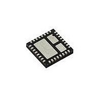
SIC417CD-T1-E3 Vishay, SIC417CD-T1-E3 Datasheet - Page 2

SIC417CD-T1-E3
Manufacturer Part Number
SIC417CD-T1-E3
Description
IC DRIVER MOSF SYNC BUCK 55MLPQ
Manufacturer
Vishay
Series
microBUCK™r
Datasheet
1.SIC417CD-T1-E3.pdf
(20 pages)
Specifications of SIC417CD-T1-E3
Topology
Step-Down (Buck) Synchronous (1), Linear (LDO) (1)
Function
Any Function
Number Of Outputs
2
Frequency - Switching
200kHz ~ 1MHz
Voltage/current - Output 1
0.5 V ~ 5.5 V, 10A
Voltage/current - Output 2
0.75 V ~ 5.25 V, 150mA
W/led Driver
No
W/supervisor
No
W/sequencer
No
Voltage - Supply
3 V ~ 28 V
Operating Temperature
-25°C ~ 125°C
Mounting Type
*
Package / Case
*
Output Voltage
0.5 V to 5.5 V
Output Current
10 A
Input Voltage
3 V to 28 V
Switching Frequency
200 KHz to 1 MHz
Mounting Style
SMD/SMT
Duty Cycle (max)
95 %
Primary Input Voltage
28V
No. Of Outputs
1
Voltage Regulator Case Style
MLPQ
No. Of Pins
32
Operating Temperature Range
-25°C To +125°C
Svhc
No SVHC
Rohs Compliant
Yes
Lead Free Status / RoHS Status
Lead free / RoHS Compliant
Lead Free Status / RoHS Status
Lead free / RoHS Compliant, Lead free / RoHS Compliant
Available stocks
Company
Part Number
Manufacturer
Quantity
Price
Part Number:
SIC417CD-T1-E3
Manufacturer:
VISHAY/威世
Quantity:
20 000
SiC417
Vishay Siliconix
PIN CONFIGURATION
www.vishay.com
2
6, 9 - 11, PAD 2
PIN DESCRIPTION
13, 23 - 25, 28,
ORDERING INFORMATION
Pin Number
4, 30, PAD 1
PAD 3
15-22
12
14
26
27
29
31
32
1
2
3
5
7
8
Symbol
EN/PSV
P
A
P
V
V
BST
ENL
FBL
V5V
GOOD
I
V
t
DH
FB
DL
LX
GND
OUT
GND
LIM
LDO
ON
IN
SiC417CD-T1-E3
Part Number
SiC417DB
Feedback input for switching regulator. Connect to an external resistor divider from output to program the
output voltage.
Feedback input for the LDO. Connect to an external resistor divider from V
5 V power input for internal analog circuits and gate drives. Connect to external 5 V supply or configure the
LDO for 5 V and connect to V
Analog ground.
Output voltage input to the SiC417. Additionally, may be used to bypass LDO to supply V
Input supply voltage.
LDO output.
Bootstrap pin. A capacitor is connected between BST to LX to develop the floating voltage for the high-side
gate drive.
High-side gate drive - do not connect this pin.
Low-side gate drive - do not connect this pin.
Switching (Phase) node.
Power ground.
Open-drain power good indicator. High impedance indicates power is good. An external pull-up resistor is
required.
Current limit sense point - to program the current limit connect a resistor from I
Tri-state pin. Enable input for switching regulator. Connect EN to A
Float pin for forced continuous and pull high for power-save mode.
On-time set input. Set the on-time by a series resistor to the input supply voltage.
Enable input for the LDO. Connect ENL to A
A
V
V
V5V
BST
FBL
GND
OUT
LDO
V
FB
IN
A
PAD 2
V
PAD 1
GND
IN
35
LDO
34
.
PAD 3
LX 33
GND
Description
to disable the LDO.
LX
LX
P
P
P
P
P
P
GND
GND
GND
GND
GND
GND
Evaluation board
MLPQ55-32
GND
Package
to disable the switching regulator.
LDO
LIM
to program the V
S10-1367-Rev. D, 14-Jun-10
Document Number: 69062
to LX.
LDO
directly.
LDO
output.


