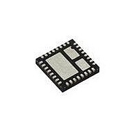
SIC417CD-T1-E3 Vishay, SIC417CD-T1-E3 Datasheet - Page 8

SIC417CD-T1-E3
Manufacturer Part Number
SIC417CD-T1-E3
Description
IC DRIVER MOSF SYNC BUCK 55MLPQ
Manufacturer
Vishay
Series
microBUCK™r
Datasheet
1.SIC417CD-T1-E3.pdf
(20 pages)
Specifications of SIC417CD-T1-E3
Topology
Step-Down (Buck) Synchronous (1), Linear (LDO) (1)
Function
Any Function
Number Of Outputs
2
Frequency - Switching
200kHz ~ 1MHz
Voltage/current - Output 1
0.5 V ~ 5.5 V, 10A
Voltage/current - Output 2
0.75 V ~ 5.25 V, 150mA
W/led Driver
No
W/supervisor
No
W/sequencer
No
Voltage - Supply
3 V ~ 28 V
Operating Temperature
-25°C ~ 125°C
Mounting Type
*
Package / Case
*
Output Voltage
0.5 V to 5.5 V
Output Current
10 A
Input Voltage
3 V to 28 V
Switching Frequency
200 KHz to 1 MHz
Mounting Style
SMD/SMT
Duty Cycle (max)
95 %
Primary Input Voltage
28V
No. Of Outputs
1
Voltage Regulator Case Style
MLPQ
No. Of Pins
32
Operating Temperature Range
-25°C To +125°C
Svhc
No SVHC
Rohs Compliant
Yes
Lead Free Status / RoHS Status
Lead free / RoHS Compliant
Lead Free Status / RoHS Status
Lead free / RoHS Compliant, Lead free / RoHS Compliant
Available stocks
Company
Part Number
Manufacturer
Quantity
Price
Part Number:
SIC417CD-T1-E3
Manufacturer:
VISHAY/威世
Quantity:
20 000
SiC417
Vishay Siliconix
On-Time One-Shot Generator (t
Frequency
The SiC417 have an internal on-time one-shot generator
which is a comparator that has two inputs. The FB
Comparator output goes high when VFB is less than the
internal 500 mV reference. This feeds into the gate drive and
turns on the high-side MOSFET, and also starts the one-shot
timer. The one-shot timer uses an internal comparator and a
capacitor. One comparator input is connected to V
other input is connected to the capacitor. When the on-time
begins, the internal capacitor charges from zero volts
through a current which is proportional to V
capacitor voltage reaches V
and the high-side MOSFET turns off. The figure 2 shows the
on-chip implementation of on-time generation.
This method automatically produces an on-time that is
proportional to V
steady-state conditions, the switching frequency can be
determined from the on-time by the following equation.
The SiC417 uses an external resistor to set the ontime which
indirectly sets the frequency. The on-time can be
programmed to provide operating frequency from 200 kHz to
1 MHz using a resistor between the t
resistor value is selected by the following equation.
The maximum R
equation.
V
The switcher output voltage is regulated by comparing V
as seen through a resistor divider at the FB pin to the internal
500 mV reference voltage, see figure 3.
www.vishay.com
8
V
OUT
FB
500 mV
V
R
IN
OUT
ton
Voltage Selection
FB comparator
On-time = K x R
-
+
One-shot
timer
Figure 2 - On-Time Generation
R
OUT
TON
ton
=
R
and inversely proportional to V
value allowed is shown by the following
ton
ton_MAX
(t
f
ON
SW
x (V
25 pF x V
- 10 ns) x V
=
drives
Gate
OUT/
DH
t
DL
ON
=
V
OUT
V
OUT
V
IN
x V
15 µA
IN_MIN
OUT
)
, the on-time is completed
IN
IN
Q1
Q1
V
Q2
ON
LX
ON
C
pin and ground. The
) and Operating
OUT
ESR
L
+
IN
. When the
IN
OUT
V
. Under
FB
OUT
, the
OUT
As the control method regulates the valley of the output ripple
voltage, the DC output voltage V
ripple according to the following equation.
V
Enable and Power-Save Inputs
The EN/PSV and ENL inputs are used to enable or disable
the switching regulator and the LDO.
When EN/PSV is low (grounded), the switching regulator is
off and in its lowest power state. When off, the output of the
switching regulator soft-discharges the output into a 15 Ω
internal resistor via the V
When EN/PSV is allowed to float, the pin voltage will fl oat to
1.5 V. The switching regulator turns on with power-save
disabled and all switching is in forced continuous mode.
When EN/PSV is high (above 2.0 V), the switching regulator
turns on with ultra-sonic power-save enabled. The SiC417
ultra-sonic power-save operation maintains a minimum
switching frequency of 25 kHz, for applications with stringent
audio requirements.
The ENL input is used to control the internal LDO. This input
serves a second function by acting as a V
the switching regulator.
The LDO is off when ENL is low (grounded). When ENL is a
logic high but below the V
then the LDO is on and the switcher is off. When ENL is
above the V
switcher is also enabled if the EN/PSV pin is not grounded.
Forced Continuous Mode Operation
The SiC417 operates the switcher in Forced Continuous
Mode (FCM) by floating the EN/PSV pin (see figure 4). In this
mode one of the power MOSFETs is always on, with no
intentional dead time other than to avoid cross-conduction.
This feature results in uniform frequency across the full load
range with the trade-off being poor efficiency at light loads
due to the high-frequency switching of the MOSFETs.
OUT
V
OUT
= 0.5 x (1 + R
IN UVLO
Figure 3 - Output Voltage Selection
1
/R
threshold, the LDO is enabled and the
2
) + V
R
OUT
1
IN UVLO
RIPPLE
pin.
R
OUT
2
S10-1367-Rev. D, 14-Jun-10
threshold (2.6 V typical),
/2
Document Number: 69062
is off set by the output
IN UVLO
To FB pin
sensor for


