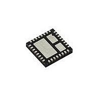
SIC417CD-T1-E3 Vishay, SIC417CD-T1-E3 Datasheet - Page 3

SIC417CD-T1-E3
Manufacturer Part Number
SIC417CD-T1-E3
Description
IC DRIVER MOSF SYNC BUCK 55MLPQ
Manufacturer
Vishay
Series
microBUCK™r
Datasheet
1.SIC417CD-T1-E3.pdf
(20 pages)
Specifications of SIC417CD-T1-E3
Topology
Step-Down (Buck) Synchronous (1), Linear (LDO) (1)
Function
Any Function
Number Of Outputs
2
Frequency - Switching
200kHz ~ 1MHz
Voltage/current - Output 1
0.5 V ~ 5.5 V, 10A
Voltage/current - Output 2
0.75 V ~ 5.25 V, 150mA
W/led Driver
No
W/supervisor
No
W/sequencer
No
Voltage - Supply
3 V ~ 28 V
Operating Temperature
-25°C ~ 125°C
Mounting Type
*
Package / Case
*
Output Voltage
0.5 V to 5.5 V
Output Current
10 A
Input Voltage
3 V to 28 V
Switching Frequency
200 KHz to 1 MHz
Mounting Style
SMD/SMT
Duty Cycle (max)
95 %
Primary Input Voltage
28V
No. Of Outputs
1
Voltage Regulator Case Style
MLPQ
No. Of Pins
32
Operating Temperature Range
-25°C To +125°C
Svhc
No SVHC
Rohs Compliant
Yes
Lead Free Status / RoHS Status
Lead free / RoHS Compliant
Lead Free Status / RoHS Status
Lead free / RoHS Compliant, Lead free / RoHS Compliant
Available stocks
Company
Part Number
Manufacturer
Quantity
Price
Part Number:
SIC417CD-T1-E3
Manufacturer:
VISHAY/威世
Quantity:
20 000
FUNCTIONAL BLOCK DIAGRAM
Stresses beyond those listed under "Absolute Maximum Ratings" may cause permanent damage to the device. These are stress ratings only,
and functional operation of the device at these or any other conditions beyond those indicated in the operational sections of the specifications is
not implied. Exposure to absolute maximum rating/conditions for extended periods may affect device reliability.
Note:
For proper operation, the device should be used within the recommended conditions.
Document Number: 69062
S10-1367-Rev. D, 14-Jun-10
ABSOLUTE MAXIMUM RATINGS T
Parameter
LX to P
LX to P
V
V
BST Bootstrap to LX; V5V to P
A
EN/PSV, P
t
BST to P
RECOMMENDED OPERATING CONDITIONS
Parameter
Input Voltage
V5V to P
V
THERMAL RESISTANCE RATINGS
Parameter
Storage Temperature
Maximum Junction Temperature
Operation Junction Temperature
ON
IN
EN
GND
OUT
to P
to P
Maximum Voltage
to P
to P
GND
GND
GND
GND
GND
GND
GND
GND
GOOD
Voltage
Voltage (transient - 100 ns)
Voltage
, I
31
1.20.21
1
2
PAD 1
5
7
LIM
A
GND
FB
t
FBL
V
V
ON
OUT
LDO
, V
OUT
V5V
, V
Bypass Comparator
Reference
Soft Start
LDO
GND
FB Comparator
3
Y
V5V
, FB, FBL to GND
A
B
MUX
+
-
PGD
Control and Status
26
LDO
Symbol
A
V
V5V
V
= 25 °C, unless otherwise noted
OUT
EN/PSV
IN
32
Symbol
V
ENL
IN
29
T
STG
T
T
Valley 1 - Limit
Zero Cross
J
J
Detector
Gate Drive
Control
V5V
Symbol
V
AG-PG
V
V
V
V
Min.
3.0
4.5
0.5
EN
LX
LX
IN
DL
Min.
- 40
- 25
-
V5V
Typ.
Min.
- 0.3
- 0.3
- 0.3
- 0.3
- 0.3
- 0.3
- 0.3
- 0.3
- 2
Typ.
6, 9 - 11 PAD 3
V
IN
+ (V5V + 0.3)
+ (V5V - 1.5)
V
Max.
Max.
+ 6.0
+ 0.3
+ 30
+ 30
+ 30
+ 35
5.5
5.5
IN
28
V
+ 150
+ 125
Max.
150
Vishay Siliconix
IN
13, 23 - 25
28, PAD 3
P
BST
GND
I
LIM
LX
15-22
27
8
www.vishay.com
SiC417
Unit
Unit
Unit
V
V
°C
3


