SI270X-A-EVB Silicon Laboratories Inc, SI270X-A-EVB Datasheet - Page 23
SI270X-A-EVB
Manufacturer Part Number
SI270X-A-EVB
Description
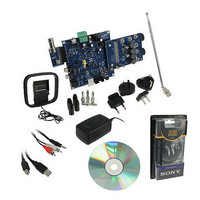
BOARD EVAL FOR SI270X-A
Manufacturer
Silicon Laboratories Inc
Datasheet
1.SI2704-A10-GM.pdf
(46 pages)
Specifications of SI270X-A-EVB
Board Type
Fully Populated
Amplifier Type
Class D
Output Type
2-Channel (Stereo) with Stereo Headphones
Max Output Power X Channels @ Load
5W x 2 @ 3 Ohm
Voltage - Supply
9V
Utilized Ic / Part
SI270X-A
Description/function
Audio Amplifiers
Output Power
5 W
Product
Audio Modules
For Use With/related Products
Si270x
Lead Free Status / RoHS Status
Lead free / RoHS Compliant
Operating Temperature
-
Lead Free Status / Rohs Status
Lead free / RoHS Compliant
Other names
336-1929


Si2704/05/06/07-A10
R1
Audio Left
OUTSEL
Audio Right
R2
Figure 16. Headphone Plug Detection Application Schematic
4.4. Clocking
A low jitter on-chip PLL synchronizes to an external clock reference and generates all necessary internal clocks.
2
Three options are available for the external reference: a crystal, a reference clock or the digital I
S audio bit clock.
In addition, a buffered user-programmable output clock can be generated on the CLKO pin for use as a clock
reference for external circuits.
4.4.1. Reference Clock Input
Using an external crystal, the on-chip crystal oscillator generates a precise, low jitter internal clock reference for the
best audio performance.
For system design flexibility, the device also supports the options to use either an external reference clock or the
2
I
S bit clock as the PLL reference. Noise performance of the amplifier is a direct function of the jitter characteristics
of the external source.
The source of the external reference is programmed using the CLOCK_SOURCE property through the 2-Wire
interface.
4.4.1.1. Crystal Oscillator Operation
When a crystal is connected between XTLI and XTLO pins and the chip is configured properly all the timing for the
chip is derived from the on-chip crystal oscillator.
A range of crystals are supported and the device needs to be programmed to the selected frequency using the
CLOCK_REF_FREQ property. The crystal oscillator provides the best audio performance.
4.4.1.2. External Reference Clock Operation
In this mode, the device operates in slave clock mode and the reference clock is provided by an external clock
source on pin XTLI. A wide range of input clock frequencies are supported in this mode ranging from 2.048 to
49 MHz. Refer to Table 11 on page 12 or to the “AN469: Si270x Programming Guide” for more information on the
complete range of frequencies and settings required for operation on this mode.
2
4.4.1.3. I
S Reference Clock Operation
2
The device can operate in slave clock mode using the DCLK signal from the I
S bus as a timing reference. In this
2
mode the device needs to be programmed for one of the supported I
S clock rates and pin XTLI should be
connected to ground.
4.4.2. Reference Clock Output
The Si2704/05/06/07 may provide a buffered output clock to be used as reference for external circuits when the
chip is programmed for either Active or Standby mode. The clock output frequency and synchronization source is
programmable.
The Si270x supports a number of reference clock frequencies that are related to the PWM switching rate. These
CLKO output frequencies can be especially useful for synchronizing the amplifier to switching power supplies.
Refer to the “AN469: Si270x Programming Guide” for more information on the settings requested for operation.
Rev. 0.6
23
Related parts for SI270X-A-EVB
Image
Part Number
Description
Manufacturer
Datasheet
Request
R

Part Number:
Description:
SMD/C°/SINGLE-ENDED OUTPUT SILICON OSCILLATOR
Manufacturer:
Silicon Laboratories Inc
Part Number:
Description:
Manufacturer:
Silicon Laboratories Inc
Datasheet:
Part Number:
Description:
N/A N/A/SI4010 AES KEYFOB DEMO WITH LCD RX
Manufacturer:
Silicon Laboratories Inc
Datasheet:
Part Number:
Description:
N/A N/A/SI4010 SIMPLIFIED KEY FOB DEMO WITH LED RX
Manufacturer:
Silicon Laboratories Inc
Datasheet:
Part Number:
Description:
N/A/-40 TO 85 OC/EZLINK MODULE; F930/4432 HIGH BAND (REV E/B1)
Manufacturer:
Silicon Laboratories Inc
Part Number:
Description:
EZLink Module; F930/4432 Low Band (rev e/B1)
Manufacturer:
Silicon Laboratories Inc
Part Number:
Description:
I°/4460 10 DBM RADIO TEST CARD 434 MHZ
Manufacturer:
Silicon Laboratories Inc
Part Number:
Description:
I°/4461 14 DBM RADIO TEST CARD 868 MHZ
Manufacturer:
Silicon Laboratories Inc
Part Number:
Description:
I°/4463 20 DBM RFSWITCH RADIO TEST CARD 460 MHZ
Manufacturer:
Silicon Laboratories Inc
Part Number:
Description:
I°/4463 20 DBM RADIO TEST CARD 868 MHZ
Manufacturer:
Silicon Laboratories Inc
Part Number:
Description:
I°/4463 27 DBM RADIO TEST CARD 868 MHZ
Manufacturer:
Silicon Laboratories Inc
Part Number:
Description:
I°/4463 SKYWORKS 30 DBM RADIO TEST CARD 915 MHZ
Manufacturer:
Silicon Laboratories Inc
Part Number:
Description:
N/A N/A/-40 TO 85 OC/4463 RFMD 30 DBM RADIO TEST CARD 915 MHZ
Manufacturer:
Silicon Laboratories Inc
Part Number:
Description:
I°/4463 20 DBM RADIO TEST CARD 169 MHZ
Manufacturer:
Silicon Laboratories Inc