SI270X-A-EVB Silicon Laboratories Inc, SI270X-A-EVB Datasheet - Page 34
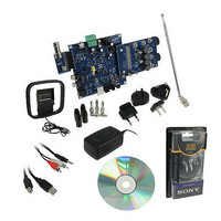
SI270X-A-EVB
Manufacturer Part Number
SI270X-A-EVB
Description
BOARD EVAL FOR SI270X-A
Manufacturer
Silicon Laboratories Inc
Datasheet
1.SI2704-A10-GM.pdf
(46 pages)
Specifications of SI270X-A-EVB
Board Type
Fully Populated
Amplifier Type
Class D
Output Type
2-Channel (Stereo) with Stereo Headphones
Max Output Power X Channels @ Load
5W x 2 @ 3 Ohm
Voltage - Supply
9V
Utilized Ic / Part
SI270X-A
Description/function
Audio Amplifiers
Output Power
5 W
Product
Audio Modules
For Use With/related Products
Si270x
Lead Free Status / RoHS Status
Lead free / RoHS Compliant
Operating Temperature
-
Lead Free Status / Rohs Status
Lead free / RoHS Compliant
Other names
336-1929


Si2704/05/06/07-A10
6. Pin Descriptions
6.1. 24-Pin QFN Package
34
Pin Number
GND PAD
10
11
12
13
14
15
16
17
18
19
20
21
22
23
24
1
2
3
4
5
6
7
8
9
OUTSEL/MFP2
AUXOR
OUTPR
OUTNR
AUXOL
OUTNL
OUTPL
GNDR
Name
CLKO
VPPR
GNDL
DCLK
SCLK
MFP3
MFP1
VPPL
XTLO
SDIO
GND
XTLI
VDD
RST
DFS
DIN
VIO
Low voltage ground for VDD. Connect to PCB ground plane.
I
I
I/O supply voltage.
Serial clock input for I
Serial data input/output for I
Buffered reference clock output. Configures 2-Wire address on RST.
Multi-function pin 3.
PWMDAC left channel analog output on Si2705/07 (Reserved on Si2704/06).
PWMDAC right channel analog output on Si2705/07 (Reserved on Si2704/06).
Multi-function pin 1.
Output select three-level control input: 2.0, 2.1 or line out mode.
Right channel power stage supply voltage.
Right channel power stage “P” output.
Right channel power stage “N” output.
Right channel power stage ground.
Left channel power stage ground.
Left channel power stage “N” output.
Left channel power stage “P” output.
Left channel power stage supply voltage.
Device reset (active low) input.
External crystal output.
Reference clock or external crystal input.
Low voltage supply voltage.
I
2
2
2
S digital I/O data clock.
S digital data input port.
S digital I/O data frame synch.
Figure 25. Pin Configuration
DCLK
CLKO
Table 18. Pin Descriptions
SCLK
SDIO
DIN
VIO
1
2
3
4
5
6
24
7
24-Pin QFN Package
23
8
Top Down View
Rev. 0.6
(Back Paddle)
GND PAD
22
9
21
10
2
C-compliant 2-Wire control interface.
20
11
19
12
2
C-compliant 2-Wire control interface.
18
17
16
15
14
13
OUTPL
OUTNL
GNDL
GNDR
OUTNR
OUTPR
Function
Related parts for SI270X-A-EVB
Image
Part Number
Description
Manufacturer
Datasheet
Request
R

Part Number:
Description:
SMD/C°/SINGLE-ENDED OUTPUT SILICON OSCILLATOR
Manufacturer:
Silicon Laboratories Inc
Part Number:
Description:
Manufacturer:
Silicon Laboratories Inc
Datasheet:
Part Number:
Description:
N/A N/A/SI4010 AES KEYFOB DEMO WITH LCD RX
Manufacturer:
Silicon Laboratories Inc
Datasheet:
Part Number:
Description:
N/A N/A/SI4010 SIMPLIFIED KEY FOB DEMO WITH LED RX
Manufacturer:
Silicon Laboratories Inc
Datasheet:
Part Number:
Description:
N/A/-40 TO 85 OC/EZLINK MODULE; F930/4432 HIGH BAND (REV E/B1)
Manufacturer:
Silicon Laboratories Inc
Part Number:
Description:
EZLink Module; F930/4432 Low Band (rev e/B1)
Manufacturer:
Silicon Laboratories Inc
Part Number:
Description:
I°/4460 10 DBM RADIO TEST CARD 434 MHZ
Manufacturer:
Silicon Laboratories Inc
Part Number:
Description:
I°/4461 14 DBM RADIO TEST CARD 868 MHZ
Manufacturer:
Silicon Laboratories Inc
Part Number:
Description:
I°/4463 20 DBM RFSWITCH RADIO TEST CARD 460 MHZ
Manufacturer:
Silicon Laboratories Inc
Part Number:
Description:
I°/4463 20 DBM RADIO TEST CARD 868 MHZ
Manufacturer:
Silicon Laboratories Inc
Part Number:
Description:
I°/4463 27 DBM RADIO TEST CARD 868 MHZ
Manufacturer:
Silicon Laboratories Inc
Part Number:
Description:
I°/4463 SKYWORKS 30 DBM RADIO TEST CARD 915 MHZ
Manufacturer:
Silicon Laboratories Inc
Part Number:
Description:
N/A N/A/-40 TO 85 OC/4463 RFMD 30 DBM RADIO TEST CARD 915 MHZ
Manufacturer:
Silicon Laboratories Inc
Part Number:
Description:
I°/4463 20 DBM RADIO TEST CARD 169 MHZ
Manufacturer:
Silicon Laboratories Inc