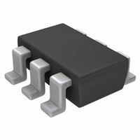
FDC6020C_F077 Fairchild Semiconductor, FDC6020C_F077 Datasheet - Page 2

FDC6020C_F077
Manufacturer Part Number
FDC6020C_F077
Description
MOSFET N P-CH 20V 6-SSOP
Manufacturer
Fairchild Semiconductor
Series
PowerTrench®r
Datasheet
1.FDC6020C_F077.pdf
(9 pages)
Specifications of FDC6020C_F077
Fet Type
N and P-Channel
Fet Feature
Logic Level Gate
Rds On (max) @ Id, Vgs
27 mOhm @ 5.9A, 4.5V
Drain To Source Voltage (vdss)
20V
Current - Continuous Drain (id) @ 25° C
5.9A, 4.2A
Vgs(th) (max) @ Id
1.5V @ 250µA
Gate Charge (qg) @ Vgs
8nC @ 4.5V
Input Capacitance (ciss) @ Vds
677pF @ 10V
Power - Max
1.2W
Mounting Type
Surface Mount
Package / Case
6-SSOT FLMP, SuperSOT-6 FLMP
Configuration
Dual Dual Source
Transistor Polarity
N and P-Channel
Resistance Drain-source Rds (on)
0.027 Ohm @ 4.5 V @ N Channel
Drain-source Breakdown Voltage
20 V
Gate-source Breakdown Voltage
+/- 12 V
Continuous Drain Current
5.9 A @ N Channel or 4.2 A @ P Channel
Power Dissipation
1800 mW
Maximum Operating Temperature
+ 150 C
Mounting Style
SMD/SMT
Minimum Operating Temperature
- 55 C
Lead Free Status / RoHS Status
Lead free / RoHS Compliant
Available stocks
Company
Part Number
Manufacturer
Quantity
Price
Company:
Part Number:
FDC6020C_F077
Manufacturer:
Fairchild Semiconductor
Quantity:
42 544
V
∆V
R
g
C
C
C
Switching Characteristics
t
t
t
t
Q
Q
Q
BV
∆BV
I
I
R
d(on)
r
d(off)
f
Electrical Characteristics
Off Characteristics
DSS
GSS
On Characteristics
Dynamic Characteristics
Symbol
FS
GS(th)
∆T
DS(on)
iss
oss
rss
g
gs
gd
∆T
G
GS(th)
DSS
J
DSS
J
Drain-Source Breakdown
Voltage
Breakdown Voltage
Temperature Coefficient
Zero Gate Voltage Drain
Current
Gate-Body Leakage
Gate Threshold Voltage
Gate Threshold Voltage
Temperature Coefficient
Static Drain-Source
On-Resistance
Forward Transconductance
Input Capacitance
Output Capacitance
Reverse Transfer Capacitance
Turn-On Delay Time
Turn-On Rise Time
Turn-Off Delay Time
Turn-Off Fall Time
Total Gate Charge
Gate-Source Charge
Gate-Drain Charge
Gate Resistance
Parameter
(Note 2)
V
V
I
I
V
V
V
V
V
V
I
I
V
V
V
V
V
V
V
V
Q1:
V
Q2:
V
Q1:
V
V
Q2:
V
V
Q1:
V
Q2:
V
D
D
D
D
f = 1.0 MHz
f = 1.0 MHz
V
GS
GS
DS
DS
GS
GS
DS
DS
GS
GS
GS
GS
GS
GS
DS
DS
DS
DS
DD
GS
DD
GS
DS
DS
GS
= –250 µA, Referenced to 25°C
= 250 µA, Referenced to 25°C
= –250 µA, Referenced to 25°C
= 250 µA, Referenced to 25°C
= 0 V,
= 0 V,
= –16 V,
= 16 V,
= +12 V,
= +12 V,
= V
= V
= –4.5 V,
= –2.5 V,
= –4.5 V, I
= 4.5 V,
= 2.5 V,
= 4.5 V, I
= –5 V,
= 5 V,
= –10 V, V
= 10 V, V
= –10 V,
= –4.5 V,
= 10 V,
= 4.5V,
= –10 V,I
= 10 V, I
= 15mV,
T
Test Conditions
A
GS
GS
= 25°C unless otherwise noted
,
,
D
D
D
GS
= 5.9 A,V
D
GS
= –4.2 A,V
= 5.9 A, T
= –4.2 A,T
= 0 V,
= 0 V,
I
I
V
V
V
V
I
I
I
I
I
I
I
I
f = 1.0 MHz
I
R
I
R
D
D
D
D
D
D
D
D
D
D
D
D
GS
GS
DS
DS
GEN
GEN
= –250 µA
= 250 µA
= –250 µA
= 250 µA
= –4.2 A
= –3.4 A
= 5.9 A
= 4.9 A
= – 4.2 A
= 5.9 A
= –1 A,
= 1 A,
GS
= 0 V
= 0 V
= 0 V
= 0 V
J
= 6 Ω
= 6 Ω
GS
= 125°C
= 4.5 V
J
= –4.5V
=125°C
Type Min Typ Max Units
Q1
Q2
Q1
Q2
Q1
Q2
Q1
Q2
Q1
Q2
Q1
Q2
Q1
Q2
Q1
Q2
Q1
Q2
Q1
Q2
Q1
Q2
Q1
Q2
Q1
Q2
Q1
Q2
Q1
Q2
Q1
Q2
Q1
Q2
Q1
Q2
Q1
Q2
–0.6
–20
0.6
20
–1.0
–14
753
677
163
171
1.0
2.2
1.6
1.5
1.9
1.8
12
–3
45
65
58
23
33
31
13
23
83
91
13
11
16
26
18
14
3
8
8
7
7
6
+100
+100
–1.5
1.5
–1
55
82
73
27
39
39
23
20
16
29
42
32
52
14
10
FDC6020C RevB (W)
1
8
mV/°C
mV/°C
mΩ
µA
nA
pF
pF
pF
nC
nC
nC
ns
ns
ns
ns
Ω
V
V
S


