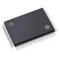
ISPPAC-CLK5610V-01T48C Lattice, ISPPAC-CLK5610V-01T48C Datasheet - Page 19

ISPPAC-CLK5610V-01T48C
Manufacturer Part Number
ISPPAC-CLK5610V-01T48C
Description
Clock Drivers & Distribution 3.3V 10-320MHz
Manufacturer
Lattice
Datasheet
1.ISPPAC-CLK5620V-01TN100C.pdf
(49 pages)
Specifications of ISPPAC-CLK5610V-01T48C
Minimum Operating Temperature
0 C
Mounting Style
SMD/SMT
Maximum Operating Temperature
70 C
Package / Case
TQFP-100
Lead Free Status / RoHS Status
Lead free / RoHS Compliant
Available stocks
Company
Part Number
Manufacturer
Quantity
Price
Company:
Part Number:
ISPPAC-CLK5610V-01T48C
Manufacturer:
Lattice Semiconductor Corporation
Quantity:
10 000
Lattice Semiconductor
Because the VCO has an operating frequency range spanning 320 MHz to 640 MHz, and the V dividers provide
division ratios from 2 to 64, the ispClock5600 can generate output signals ranging from 5MHz to 320 MHz. For per-
formance and stability reasons, however, there are several constraints which should be followed when selecting
divider values:
Output Duty Cycle
The ispClock5600’s output duty cycle varies as a function of the V divider used to generate that output. If the V-
divider setting is either 2 or a multiple of 4, the nominal output duty cycle will be exactly 50%. All other V divider set-
tings will result in non-50% output duty cycles. Table 4 summarizes the nominal output duty cycle as a function of
the V divider setting. Note that if the output is inverted, the duty cycle will be equal to 100%-DC%, where DC% is
the duty cycle indicated in the table. For example, with a V divider of 14, the non-inverted duty cycle from Table 4
will be 43%. For an inverted output, the duty cycle will be 100%-43% or 57%.
Table 4. Nominal Output Duty Cycle vs. V-divider Setting
Device Start-up Behavior
The outputs of the ispClock5600 always start up edge aligned. When the V-divider is set to a value of 2 and the out-
put skew is set to a value greater than 8, the first clock cycle immediately following power-up could be incomplete
(runt cycle). For all the remaining conditions, no runt clocks will be generated after power-up.
PLL_BYPASS Mode
The PLL_BYPASS mode is provided so that input reference signals can be coupled through to the outputs without
using the PLL functions. When PLL_BYPASS mode is enabled (PLL_BYPASS=HIGH), the output of the M divider
is routed directly to the inputs of the V dividers. In PLL_BYPASS mode, the nominal values of the V dividers are
• Use the smallest feasible value for the M divider
• The output frequency from the M (and N) divider should be greater or equal to 10 MHz.
• The product of the N divider and the V divider used to close the PLL’s feedback loop should be less than or
equal to 64 (N x V
fbk
≤ 64)
with 50% Output
Divider Settings
12
16
20
24
28
32
36
40
44
48
52
56
60
64
V
2
4
8
Duty Cycle
DC%
50
19
Non-50% Output Duty
Divider Settings with
10
14
18
22
26
30
34
38
42
46
50
54
58
62
V
6
Cycles
ispClock5600 Family Data Sheet
DC%
33
40
43
44
45
46
47
47
47
48
48
48
48
48
48


