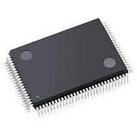
ISPPAC-CLK5610V-01T48C Lattice, ISPPAC-CLK5610V-01T48C Datasheet - Page 44

ISPPAC-CLK5610V-01T48C
Manufacturer Part Number
ISPPAC-CLK5610V-01T48C
Description
Clock Drivers & Distribution 3.3V 10-320MHz
Manufacturer
Lattice
Datasheet
1.ISPPAC-CLK5620V-01TN100C.pdf
(49 pages)
Specifications of ISPPAC-CLK5610V-01T48C
Minimum Operating Temperature
0 C
Mounting Style
SMD/SMT
Maximum Operating Temperature
70 C
Package / Case
TQFP-100
Lead Free Status / RoHS Status
Lead free / RoHS Compliant
Available stocks
Company
Part Number
Manufacturer
Quantity
Price
Company:
Part Number:
ISPPAC-CLK5610V-01T48C
Manufacturer:
Lattice Semiconductor Corporation
Quantity:
10 000
Lattice Semiconductor
ispClock5600 Family Data Sheet
GOE – Global output enable. This pin drives all outputs to a high-impedance state when it is pulled HIGH. GOE
also controls the internal feedback buffer, so that bringing GOE high will cause the PLL to lose lock.
PS0, PS1 – These input pins are used to select one of four user-defined configuration profiles for the device.
PLL_BYPASS – When this pin is pulled LOW, the V-dividers are driven from the output of the device’s VCO, and
the device behaves as a phase-locked loop. When this pin is pulled HIGH, the V-dividers are driven directly from
the output of the M-divider, and the PLL functions are effectively bypassed.
RESET – When this pin is pulled HIGH, all on-board counters are reset, and lock is lost.
TEST1,TEST2 – These pins are used for factory test functions, and should always be tied to ground.
n/c – These pins have no internal connection. We recommend that they be left unconnected.
RESERVED – These pins are reserved for factory use and should be left unconnected.
44


