BSH111,215 NXP Semiconductors, BSH111,215 Datasheet
BSH111,215
Specifications of BSH111,215
934056036215
BSH111 T/R


Related parts for BSH111,215


BSH111,215 Summary of contents
Page 1
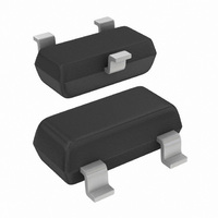
BSH111 N-channel enhancement mode field-effect transistor Rev. 02 — 26 April 2002 M3D088 1. Description N-channel enhancement mode field-effect transistor in a plastic package using TrenchMOS™ technology. Product availability: BSH111 in SOT23. 2. Features TrenchMOS™ technology Very fast switching Low ...
Page 2
Philips Semiconductors 5. Quick reference data Table 2: Quick reference data Symbol Parameter V drain-source voltage (DC drain current (DC total power dissipation tot T junction temperature j R drain-source on-state resistance DSon 6. Limiting values ...
Page 3
Philips Semiconductors 120 P der (%) 100 P tot P = ---------------------- 100% der P tot 25 C Fig 1. Normalized total power dissipation as a function of solder point temperature Limit ...
Page 4
Philips Semiconductors 7. Thermal characteristics Table 4: Thermal characteristics Symbol Parameter R thermal resistance from junction to th(j-sp) solder point R thermal resistance from junction to th(j-a) ambient 7.1 Transient thermal impedance th(j-sp) (K/ ...
Page 5
Philips Semiconductors 8. Characteristics Table 5: Characteristics unless otherwise specified j Symbol Parameter Static characteristics V drain-source breakdown (BR)DSS voltage V gate-source threshold voltage I GS(th) I drain-source leakage current DSS I gate-source leakage current GSS ...
Page 6
Philips Semiconductors Table 5: Characteristics …continued unless otherwise specified j Symbol Parameter Source-drain diode V source-drain (diode forward) SD voltage t reverse recovery time rr Q recovered charge r 9397 750 09629 Product data N-channel enhancement ...
Page 7
Philips Semiconductors 0 (A) 0.6 0.4 0 0.4 0.8 1 Fig 5. Output characteristics: drain current as a function of drain-source voltage; typical values DSon ( ) ...
Page 8
Philips Semiconductors 2 V GS(th) (V) 1.6 1.2 typ 0.8 min 0 Fig 9. Gate-source threshold voltage as a function of junction temperature. 0 ...
Page 9
Philips Semiconductors (A) 0.8 150 C 0.6 0.4 0 0.4 0 and 150 Fig 13. Source (diode forward) current as a function of source-drain ...
Page 10
Philips Semiconductors 9. Package outline Plastic surface mounted package; 3 leads DIMENSIONS (mm are the original dimensions UNIT max. 1.1 0.48 0.15 mm 0.1 0.9 0.38 0.09 OUTLINE VERSION ...
Page 11
Philips Semiconductors 10. Revision history Table 6: Revision history Rev Date CPCN Description 02 20020426 - Product data (9397 750 09629) Modifications • 20000807 - Product specification; initial version. 9397 750 09629 Product data N-channel enhancement mode ...
Page 12
Philips Semiconductors Philips Semiconductors 11. Data sheet status [1] [2] Data sheet status Product status Objective data Development Preliminary data Qualification Product data Production [1] Please consult the most recently issued data sheet before initiating or completing a design. [2] ...
Page 13
Philips Semiconductors Contents 1 Description . . . . . . . . . . . . . . . . . . . . . . . . . . . . . 1 2 Features . . . ...