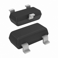
BSH111,215 NXP Semiconductors, BSH111,215 Datasheet - Page 7

BSH111,215
Manufacturer Part Number
BSH111,215
Description
MOSFET N-CH 55V 335MA SOT-23
Manufacturer
NXP Semiconductors
Series
TrenchMOS™r
Type
Power MOSFETr
Datasheet
1.BSH111215.pdf
(13 pages)
Specifications of BSH111,215
Package / Case
SOT-23-3, TO-236-3, Micro3™, SSD3, SST3
Fet Type
MOSFET N-Channel, Metal Oxide
Fet Feature
Logic Level Gate
Rds On (max) @ Id, Vgs
4 Ohm @ 500mA, 4.5V
Drain To Source Voltage (vdss)
55V
Current - Continuous Drain (id) @ 25° C
335mA
Vgs(th) (max) @ Id
1.3V @ 1mA
Gate Charge (qg) @ Vgs
1nC @ 10V
Input Capacitance (ciss) @ Vds
40pF @ 10V
Power - Max
830mW
Mounting Type
Surface Mount
Minimum Operating Temperature
- 65 C
Configuration
Single
Transistor Polarity
N-Channel
Resistance Drain-source Rds (on)
4 Ohm @ 4.5 V
Gate Charge Qg
0.05 nC
Forward Transconductance Gfs (max / Min)
380 S
Drain-source Breakdown Voltage
55 V
Gate-source Breakdown Voltage
+/- 10 V
Continuous Drain Current
0.335 A
Power Dissipation
830 mW
Maximum Operating Temperature
+ 150 C
Mounting Style
SMD/SMT
Number Of Elements
1
Polarity
N
Channel Mode
Enhancement
Drain-source On-res
4Ohm
Drain-source On-volt
55V
Gate-source Voltage (max)
±10V
Operating Temp Range
-65C to 150C
Operating Temperature Classification
Military
Mounting
Surface Mount
Pin Count
3
Package Type
TO-236AB
Lead Free Status / RoHS Status
Lead free / RoHS Compliant
Lead Free Status / RoHS Status
Lead free / RoHS Compliant, Lead free / RoHS Compliant
Other names
568-1657-2
934056036215
BSH111 T/R
934056036215
BSH111 T/R
Philips Semiconductors
9397 750 09629
Product data
Fig 5. Output characteristics: drain current as a
Fig 7. Drain-source on-state resistance as a function
R DSon
T
T
(A)
I
D
( )
j
j
0.8
0.6
= 25 C
= 25 C
0.4
0.2
16
20
12
function of drain-source voltage; typical values.
of drain current; typical values.
0
8
4
0
0
0
1.4 V
1.6 V
1.8 V
0.4
0.2
2 V
0.8
3 V
0.4
1.2
V GS = 4.5 V
V GS = 4.5 V
0.6
1.6
V DS (V)
I D (A)
03aa73
1.8 V
1.6 V
1.4 V
3 V
03aa74
2 V
0.8
2
Rev. 02 — 26 April 2002
N-channel enhancement mode field-effect transistor
Fig 6. Transfer characteristics: drain current as a
Fig 8. Normalized drain-source on-state resistance
(A)
I D
a
T
a
j
2.4
1.8
= 25 C and 150 C; V
=
1.2
0.6
0.6
0.4
0.2
0.8
function of gate-source voltage; typical values.
factor as a function of junction temperature.
0
0
--------------------------- -
R
-60
DSon 25 C
0
R
DSon
1
0
2
© Koninklijke Philips Electronics N.V. 2002. All rights reserved.
DS
T j = 25 C
60
I
D
3
R
DSon
150 C
120
4
T j ( C)
BSH111
V GS (V)
03aa75
180
5
7 of 13


