TPCF8102(TE85L,F) Toshiba, TPCF8102(TE85L,F) Datasheet
TPCF8102(TE85L,F)
Specifications of TPCF8102(TE85L,F)
TPCF8102FTR


Related parts for TPCF8102(TE85L,F)


TPCF8102(TE85L,F) Summary of contents
Page 1
... Please design the appropriate reliability upon reviewing the Toshiba Semiconductor Reliability Handbook (“Handling Precautions”/Derating Concept and Methods) and individual reliability data (i.e. reliability test report and estimated failure rate, etc). ...
Page 2
Electrical Characteristics Characteristics Gate leakage current Drain cut-off current Drain-source breakdown voltage Gate threshold voltage Drain-source ON resistance Forward transfer admittance Input capacitance Reverse transfer capacitance Output capacitance Rise time Turn-on time Switching time Fall time Turn-off ...
Page 3
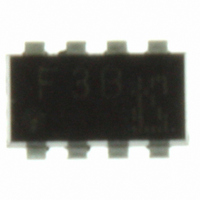
Marking (Note 5) Lot No. Lot code (month) F3B Part No. (or abbreviation code) Pin #1 Lot code A line indicates (year) lead (Pb)-free package or lead (Pb)-free finish. Note 1: Ensure that the channel temperature does not exceed 150°C. ...
Page 4
I – −5 −5 −2.5 −1.9 −1.8 −1.7 −2 −4.5 −4 −3 −4 −1.6 −3 −2 −1 −1.4 V −1 Common source Ta = 25°C Pulse test 0 −0.2 −0.4 −0.6 −0.8 0 Drain-source ...
Page 5
R – (ON) 160 Common source Pulse test 120 80 −2 −1.8 V − −1 −1.5, −2 −2 −1.5, −2.5, ...
Page 6
Safe operating area −100 I D max (pulsed)* 1 ms* −10 10 ms* −1 *: Single pulse Ta = 25°C Curves must be derated linearly with increase in temperature V DSS ...
Page 7
... The information contained herein is presented only as a guide for the applications of our products. No responsibility is assumed by TOSHIBA for any infringements of patents or other rights of the third parties which may result from its use. No license is granted by implication or otherwise under any patent or patent rights of TOSHIBA or others. • ...