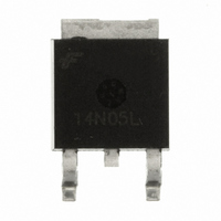
RFD14N05LSM9A Fairchild Semiconductor, RFD14N05LSM9A Datasheet

RFD14N05LSM9A
Specifications of RFD14N05LSM9A
Available stocks
Related parts for RFD14N05LSM9A
RFD14N05LSM9A Summary of contents
Page 1
... PART NUMBER PACKAGE RFD14N05L TO-251AA RFD14N05LSM TO-252AA NOTE: When ordering, use the entire part number. Add the suffix 9A to obtain the TO-252AA variant in the tape and reel, i.e., RFD14N05LSM9A. Packaging JEDEC TO-251AA DRAIN (FLANGE) ©2010 Fairchild Semiconductor Corporation RFD14N05L, RFD14N Features • ...
Page 2
... Diode Reverse Recovery Time NOTES: 2. Pulse Test: Pulse Width ≤ 300ms, Duty Cycle ≤ 2%. 3. Repetitive Rating: Pulse Width limited by max junction temperature. See Transient Thermal Impedance Curve (Figure 3) and Peak Current Capability Curve (Figure 5). ©2010 Fairchild Semiconductor Corporation Unless Otherwise Specified C ...
Page 3
... FIGURE 3. NORMALIZED MAXIMUM TRANSIENT THERMAL IMPEDANCE 100 10 OPERATION IN THIS AREA MAY BE 1 LIMITED BY r DS(ON) 0 DRAIN TO SOURCE VOLTAGE (V) DS FIGURE 4. FORWARD BIAS SAFE OPERATING AREA ©2010 Fairchild Semiconductor Corporation Unless Otherwise Specified 125 150 175 FIGURE 2. MAXIMUM CONTINUOUS DRAIN CURRENT ...
Page 4
... GATE TO SOURCE VOLTAGE (V) GS FIGURE 8. TRANSFER CHARACTERISTICS 160 V = 25V 14A 3.57Ω 140 120 100 GATE TO SOURCE RESISTANCE (Ω) GS FIGURE 10. SWITCHING TIME vs GATE RESISTANCE ©2010 Fairchild Semiconductor Corporation Unless Otherwise Specified (Continued +1] DSS 175 C = 15V 4.5 6.0 7.5 FIGURE 9. DRAIN TO SOURCE ON RESISTANCE vs GATE t d(OFF ...
Page 5
... DRAIN TO SOURCE VOLTAGE (V) DS FIGURE 14. CAPACITANCE vs DRAIN TO SOURCE VOLTAGE Test Circuits and Waveforms VARY t TO OBTAIN P R REQUIRED PEAK FIGURE 16. UNCLAMPED ENERGY TEST CIRCUIT ©2010 Fairchild Semiconductor Corporation Unless Otherwise Specified (Continued) 80 120 160 200 o C) FIGURE 13. NORMALIZED DRAIN TO SOURCE BREAKDOWN C ISS 1MHz ...
Page 6
... Test Circuits and Waveforms FIGURE 18. SWITCHING TIME TEST CIRCUIT G(REF) FIGURE 20. GATE CHARGE TEST CIRCUIT ©2010 Fairchild Semiconductor Corporation (Continued DUT DUT G(REF d(ON 90% 10% 50% PULSE WIDTH FIGURE 19. RESISTIVE SWITCHING WAVEFORMS Q g(TOT g( g(TH) FIGURE 21. GATE CHARGE WAVEFORMS RFD14N05L, RFD14N05LSM Rev. B2 ...
Page 7
... S2BMOD VSWITCH (RON = 1e-5 ROFF = 0.1 VON = 2.45 VOFF= -2.55) .ENDS NOTE: For further discussion of the PSPICE model, consult A New PSPICE Sub-circuit for the Power MOSFET Featuring Global Temperature Options; authored by William J. Hepp and C. Frank Wheatley. ©2010 Fairchild Semiconductor Corporation DPLCAP 10 RSCL2 ...
Page 8
... TRADEMARKS The following includes registered and unregistered trademarks and service marks, owned by Fairchild Semiconductor and/or its global subsidiaries, and is not intended exhaustive list of all such trademarks. AccuPower™ Auto-SPM™ Build it Now™ CorePLUS™ CorePOWER™ CROSSVOLT™ CTL™ ...


