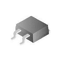
FDB8445_F085 Fairchild Semiconductor, FDB8445_F085 Datasheet

FDB8445_F085
Specifications of FDB8445_F085
Related parts for FDB8445_F085
FDB8445_F085 Summary of contents
Page 1
... Low Q Body Diode rr UIS Capability (Single Pulse/ Repetitive Pulse) Qualified to AEC Q101 RoHS Compliant GATE SOURCE TO-263AB FDB SERIES ©2006 Fairchild Semiconductor Corporation FDB8445 Rev A1 (W) ® MOSFET Applications Automotive Engine Control = 70A D Powertrain Management Solenoid and Motor Drivers Electronic Transmission ...
Page 2
Absolute Maximum Ratings Symbol V Drain to Source Voltage DSS V Gate to Source Voltage GS Drain Current Continuous ( Pulsed E Single Pulse Avalanche Energy AS Power Dissipation Derate above ...
Page 3
... This product has been designed to meet the extreme test conditions and environment demanded by the automotive industry. For a copy of the requirements, see AEC Q101 at: http://www.aecouncil.com/ All Fairchild Semiconductor products are manufactured, assembled and tested under ISO9000 and QS9000 quality systems FDB8445 Rev A1 ( 25° ...
Page 4
Typical Characteristics 1.2 1.0 0.8 0.6 0.4 0.2 0 100 T , CASE TEMPERATURE C Figure 1. Normalized Power Dissipation vs Case Temperature 2 DUTY CYCLE - DESCENDING ORDER 0.50 0.20 0.10 0.05 ...
Page 5
Typical Characteristics 1000 100 10 SINGLE PULSE = T MAX RATED OPERATION IN THIS AREA MAY BE LIMITED BY r DS(on) 0 DRAIN TO SOURCE VOLTAGE (V) DS ...
Page 6
Typical Characteristics 1.2 1.1 1.0 0.9 0.8 0.7 0.6 0.5 0.4 -80 - JUNCTION TEMPERATURE J Figure 11. Normalized Gate Threshold Voltage vs Junction Temperature 10000 1000 f = 1MHz 100 0.1 ...
Page 7
... TRADEMARKS The following are registered and unregistered trademarks Fairchild Semiconductor owns or is authorized to use and is not intended exhaustive list of all such trademarks. ® ACEx™ FAST ActiveArray™ FASTr™ Bottomless™ FPS™ Build it Now™ FRFET™ CoolFET™ ...


