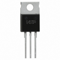
PSMN035-150P,127 NXP Semiconductors, PSMN035-150P,127 Datasheet - Page 2

PSMN035-150P,127
Manufacturer Part Number
PSMN035-150P,127
Description
MOSFET N-CH 150V 50A SOT78
Manufacturer
NXP Semiconductors
Series
TrenchMOS™r
Datasheet
1.PSMN035-150P127.pdf
(14 pages)
Specifications of PSMN035-150P,127
Package / Case
TO-220AB-3
Mounting Type
Through Hole
Power - Max
250W
Fet Type
MOSFET N-Channel, Metal Oxide
Gate Charge (qg) @ Vgs
79nC @ 10V
Vgs(th) (max) @ Id
4V @ 1mA
Current - Continuous Drain (id) @ 25° C
50A
Drain To Source Voltage (vdss)
150V
Fet Feature
Standard
Rds On (max) @ Id, Vgs
35 mOhm @ 25A, 10V
Minimum Operating Temperature
- 55 C
Configuration
Single
Transistor Polarity
N-Channel
Resistance Drain-source Rds (on)
30 mOhms
Drain-source Breakdown Voltage
150 V
Gate-source Breakdown Voltage
20 V
Continuous Drain Current
50 A
Power Dissipation
250 W
Maximum Operating Temperature
+ 175 C
Mounting Style
Through Hole
Lead Free Status / RoHS Status
Lead free / RoHS Compliant
Lead Free Status / RoHS Status
Lead free / RoHS Compliant, Lead free / RoHS Compliant
Other names
934055716127::PSMN035-150P::PSMN035-150P
5. Quick reference data
Table 2:
6. Limiting values
Table 3:
In accordance with the Absolute Maximum Rating System (IEC 60134).
Philips Semiconductors
9397 750 07994
Product specification
Symbol
V
I
P
T
R
Symbol
V
V
V
I
I
P
T
T
Source-drain diode
I
I
Avalanche ruggedness
E
I
D
D
DM
S
SM
AS
j
stg
j
DS
tot
DS
DGR
GS
tot
AS
DSon
Quick reference data
Limiting values
Parameter
drain-source voltage (DC)
drain current (DC)
total power dissipation
junction temperature
drain-source on-state resistance
Parameter
drain-source voltage (DC)
drain-gate voltage (DC)
gate-source voltage (DC)
drain current (DC)
peak drain current
total power dissipation
storage temperature
operating junction temperature
source (diode forward) current
(DC)
peak source (diode forward)
current
non-repetitive avalanche energy
non-repetitive avalanche current
Conditions
T
T
T
T
PSMN035-150B; PSMN035-150P
Rev. 04 — 22 February 2001
Conditions
T
T
T
T
T
Figure 3
T
T
T
unclamped inductive load;
I
R
T
j
mb
mb
j
AS
= 25 to 175 C
= 25 C; V
j
j
mb
mb
mb
mb
mb
mb
j
GS
= 25 to 175 C
= 25 to 175 C; R
= 25 C;
= 25 C; V
= 25 C
= 47 A; t
= 25 C;
= 100 C;
= 25 C; pulsed; t
= 25 C;
= 25 C
= 25 C; pulsed; t
= 50 ; V
Figure 4
GS
p
N-channel enhancement mode field-effect transistor
Figure 2
Figure 1
= 0.1 ms; V
GS
GS
Figure 2
= 10 V; I
= 10 V
= 10 V; starting
GS
p
p
and
= 20 k
D
and
= 25 A
DD
10 s;
10 s
3
3
50 V;
Typ
30
Min
55
55
© Philips Electronics N.V. 2001. All rights reserved.
Max
150
150
50
36
200
250
+175
+175
50
200
460
50
Max
150
50
250
175
35
20
Unit
V
V
V
A
A
A
W
A
A
mJ
A
Unit
V
A
W
m
C
C
C
2 of 14


