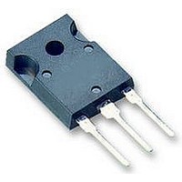
2SK3845(Q) Toshiba, 2SK3845(Q) Datasheet

MOSFET N-CH 60V 70A SC-67

2SK3845(Q)

Manufacturer Part Number
2SK3845(Q)
Description
MOSFET N-CH 60V 70A SC-67
Manufacturer
Toshiba
Datasheet

Specifications of 2SK3845(Q)

Fet Type
MOSFET N-Channel, Metal Oxide
Fet Feature
Logic Level Gate
Rds On (max) @ Id, Vgs
5.8 mOhm @ 35A, 10V
Drain To Source Voltage (vdss)
60V
Current - Continuous Drain (id) @ 25° C
70A
Vgs(th) (max) @ Id
4V @ 1mA
Gate Charge (qg) @ Vgs
196nC @ 10V
Input Capacitance (ciss) @ Vds
12400pF @ 10V
Power - Max
125W
Mounting Type
Through Hole
Package / Case
2-16C1B (TO-247 N)
Transistor Polarity
N Channel
Continuous Drain Current Id
70A
Drain Source Voltage Vds
60V
On Resistance Rds(on)
5.8mohm
Rds(on) Test Voltage Vgs
10V
Threshold Voltage Vgs Typ
4V
Rohs Compliant
Yes
Configuration
Single
Resistance Drain-source Rds (on)
0.0058 Ohms
Drain-source Breakdown Voltage
60 V
Gate-source Breakdown Voltage
+/- 20 V
Continuous Drain Current
70 A
Power Dissipation
125 W
Mounting Style
Through Hole
Minimum Operating Temperature
- 55 C
Lead Free Status / RoHS Status
Lead free / RoHS Compliant

Available stocks

Company
Part Number
Manufacturer
Quantity
Price
Part Number:
2SK3845(Q)
Manufacturer:
MOTOROLA
Quantity:
14 000
Switching Regulator, DC-DC Converter Applications and
Motor Drive Applications
Absolute Maximum Ratings
Thermal Characteristics
This transistor is an electrostatic-sensitive device. Please handle with caution.
Low drain-source ON resistance: R
High forward transfer admittance: |Y
Low leakage current: I
Enhancement model: V
Drain-source voltage
Drain-gate voltage (R
Gate-source voltage
Drain current
Drain power dissipation (Tc = 25°C)
Single pulse avalanche energy
Avalanche current
Repetitive avalanche energy (Note 3)
Channel temperature
Storage temperature range
Note:
Thermal resistance, channel to case
Thermal resistance, channel to ambient
Note 1: Ensure that the channel temperature does not exceed 150℃.
Note 2: V
Note 3: Repetitive rating: pulse width limited by maximum channel temperature
Using continuously under heavy loads (e.g. the application of high temperature/current/voltage and the significant change in
temperature, etc.) may cause this product to decrease in the reliability significantly even if the operating conditions (i.e.
operating temperature/current/voltage, etc.) are within the absolute maximum ratings. Please design the appropriate
reliability upon reviewing the Toshiba Semiconductor Reliability Handbook (“Handling Precautions”/Derating Concept and
Methods) and individual reliability data (i.e. reliability test report and estimated failure rate, etc).
Characteristics
DD
Characteristics
TOSHIBA Field Effect Transistor Silicon N Channel MOS Type (U-MOSIII)
= 25 V, T
GS
DC
Pulse (Note 1)
= 20 kΩ)
ch
DSS
th
= 25°C (initial), L = 91 µH, R
= 2.0 to 4.0 V (V
(Note 1)
(Note 2)
= 100 µA (max) (V
DS (ON)
(Ta = 25°C)
Symbol
V
V
V
fs
E
E
T
T
I
I
DGR
P
DSS
GSS
DP
AR
I
| = 88 S (typ.)
AS
AR
stg
D
ch
R
R
D
2SK3845
Symbol
th (ch-c)
th (ch-a)
DS
= 4.7 mΩ (typ.)
DS
= 10 V, I
= 60 V)
−55 to150
Rating
G
12.5
±20
280
125
328
150
60
60
70
70
D
1
= 25 Ω, I
Max
= 1 mA)
1.0
50
AR
Unit
mJ
mJ
°C/W
°C/W
°C
°C
W
= 70 A
V
V
V
A
A
Unit
Weight: 4.6 g (typ.)
JEDEC
JEITA
TOSHIBA
1. GATE
2. DRAIN (HEAT SINK)
3. SOURCE
1
2-16C1B
2006-11-17
2SK3845
2
3
Unit: mm

Related parts for 2SK3845(Q)

2SK3845(Q) Summary of contents

Page 1

... Please design the appropriate reliability upon reviewing the Toshiba Semiconductor Reliability Handbook (“Handling Precautions”/Derating Concept and Methods) and individual reliability data (i.e. reliability test report and estimated failure rate, etc). ...

Page 2

... Source-Drain Ratings and Characteristics Characteristics Continuous drain reverse current (Note 1) Pulse drain reverse current (Note 1) Forward voltage (diode) Reverse recovery time Reverse recovery charge Marking TOSHIBA K3845 Part No. (or abbreviation code) Lot No. A line indicates lead (Pb)-free package or lead (Pb)-free finish. Symbol Test Condition = ± ...

Page 3

I – 100 Common source 25°C Pulse test 0.2 0.4 0.6 0.8 Drain−source voltage V ( – V ...

Page 4

(ON) 10 Common source Pulse test −80 − 120 Case temperature Tc (°C) Capacitance – ...

Page 5

Duty = 0.5 0.2 0.1 0.1 0.05 0.02 0.01 0.01 10 µ 100 µ Safe operating area 1000 500 I D max (pulsed) * 300 100 µ max (continuous) 100 30 DC ...

Page 6

... TOSHIBA is continually working to improve the quality and reliability of its products. Nevertheless, semiconductor devices in general can malfunction or fail due to their inherent electrical sensitivity and vulnerability to physical stress the responsibility of the buyer, when utilizing TOSHIBA products, to comply with the standards of safety in making a safe design for the entire system, and to avoid situations in which a malfunction or failure of such TOSHIBA products could cause loss of human life, bodily injury or damage to property ...

Related keywords