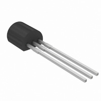
BF245C,112 NXP Semiconductors, BF245C,112 Datasheet

BF245C,112
Specifications of BF245C,112
Related parts for BF245C,112
BF245C,112 Summary of contents
Page 1
DATA SHEET BF245A; BF245B; BF245C N-channel silicon field-effect transistors Product specification Supersedes data of April 1995 DISCRETE SEMICONDUCTORS 1996 Jul 30 ...
Page 2
... NXP Semiconductors N-channel silicon field-effect transistors FEATURES Interchangeability of drain and source connections Frequencies up to 700 MHz. APPLICATIONS LF, HF and DC amplifiers. DESCRIPTION General purpose N-channel symmetrical junction field-effect transistors in a plastic TO-92 variant package. CAUTION The device is supplied in an antistatic package. The gate-source input must be protected against static discharge during transport or handling ...
Page 3
... NXP Semiconductors N-channel silicon field-effect transistors LIMITING VALUES In accordance with the Absolute Maximum Rating System (IEC 134). SYMBOL PARAMETER V drain-source voltage DS V gate-drain voltage GDO V gate-source voltage GSO I drain current D I gate current G P total power dissipation tot T storage temperature stg ...
Page 4
... NXP Semiconductors N-channel silicon field-effect transistors DYNAMIC CHARACTERISTICS = 25 C; unless otherwise specified. Common source; T amb SYMBOL PARAMETER C input capacitance is C reverse transfer capacitance rs C output capacitance os g input conductance is g output conductance os y forward transfer admittance fs y reverse transfer admittance rs ...
Page 5
... NXP Semiconductors N-channel silicon field-effect transistors 6 handbook, halfpage I D (mA Fig.4 Output characteristics for BF245A; typical values. 15 handbook, halfpage I D (mA Fig.6 Output characteristics for BF245B; typical values. 1996 Jul 30 MBH555 handbook, halfpage −0.5 V −1 V −1 ( MBH553 handbook, halfpage −0.5 V −1 V − ...
Page 6
... NXP Semiconductors N-channel silicon field-effect transistors 30 handbook, halfpage I D (mA Fig.8 Output characteristics for BF245C; typical values. 15 handbook, halfpage I D (mA Fig.10 Drain current as a function of junction temperature; typical values for BF245B. 1996 Jul 30 MBH554 handbook, halfpage −1 V −2 V −3 V − ( Fig.9 ...
Page 7
... NXP Semiconductors N-channel silicon field-effect transistors 3 10 handbook, halfpage g is (μA/ amb Fig.12 Input admittance; typical values handbook, halfpage −b fs (mA/ − amb Fig.14 Common-source forward transfer admittance as a function of frequency; typical values. 1996 Jul 30 MGE778 2 10 handbook, halfpage ...
Page 8
... NXP Semiconductors N-channel silicon field-effect transistors 6 handbook, halfpage C is (pF) 4 typ 2 0 −2 − MHz amb Fig.16 Input capacitance as a function of gate-source voltage; typical values. 8 handbook, halfpage | (mA/V) BF245B 6 BF245A kHz amb Fig.18 Forward transfer admittance as a function of drain current; typical values. ...
Page 9
... NXP Semiconductors N-channel silicon field-effect transistors 3 10 handbook, halfpage R DSon (kΩ BF245A 1 −1 10 −1 − kHz amb Fig.20 Drain-source on-state resistance as a function of gate-source voltage; typical values. 1996 Jul 30 MGE790 handbook, halfpage BF245B BF245C −3 − (V) 9 BF245A; BF245B; BF245C ...
Page 10
... NXP Semiconductors N-channel silicon field-effect transistors PACKAGE OUTLINE Plastic single-ended leaded (through hole) package; 3 leads (on-circle DIMENSIONS (mm are the original dimensions) UNIT 5.2 0.48 0.66 0.45 mm 5.0 0.40 0.55 0.38 Note 1. Terminal dimensions within this zone are uncontrolled to allow for flow of plastic and terminal irregularities. ...
Page 11
... In no event shall NXP Semiconductors be liable for any indirect, incidental, punitive, special or consequential damages (including - without limitation - lost profits, lost savings, business interruption, costs related to the ...
Page 12
... NXP Semiconductors’ specifications such use shall be solely at customer’s own risk, and (c) customer fully indemnifies NXP Semiconductors for any liability, damages or failed product claims resulting from customer design and use of the product for automotive applications beyond NXP Semiconductors’ ...
Page 13
... Interface, Security and Digital Processing expertise Customer notification This data sheet was changed to reflect the new company name NXP Semiconductors, including new legal definitions and disclaimers. No changes were made to the technical content, except for package outline drawings which were updated to the latest version. ...


