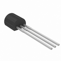
BF245C,112 NXP Semiconductors, BF245C,112 Datasheet - Page 8

BF245C,112
Manufacturer Part Number
BF245C,112
Description
JFET N-CH 30V 25MA TO-92
Manufacturer
NXP Semiconductors
Datasheet
1.BF245C112.pdf
(13 pages)
Specifications of BF245C,112
Package / Case
TO-92-3 (Standard Body), TO-226
Current Rating
25mA
Frequency
100MHz
Transistor Type
N-Channel JFET
Noise Figure
1.5dB
Voltage - Test
15V
Configuration
Single
Minimum Operating Temperature
- 65 C
Mounting Style
Through Hole
Transistor Polarity
N-Channel
Drain Source Voltage Vds
30 V
Gate-source Cutoff Voltage
- 0.25 V to - 8 V
Gate-source Breakdown Voltage
- 30 V
Maximum Drain Gate Voltage
- 30 V
Continuous Drain Current
25 mA
Drain Current (idss At Vgs=0)
12 mA to 25 mA
Power Dissipation
300 mW
Maximum Operating Temperature
+ 150 C
Lead Free Status / RoHS Status
Lead free / RoHS Compliant
Power - Output
-
Gain
-
Current - Test
-
Lead Free Status / Rohs Status
Lead free / RoHS Compliant
Other names
933106600112::BF245CP::BF245CP
NXP Semiconductors
1996 Jul 30
handbook, halfpage
handbook, halfpage
N-channel silicon field-effect transistors
Fig.18 Forward transfer admittance as a function of
V
V
DS
DS
(mA/V)
(pF)
C is
|y fs |
= 20 V; f = 1 MHz; T
= 15 V; f = 1 kHz; T
Fig.16 Input capacitance as a function of
8
6
4
2
0
6
4
2
0
drain current; typical values.
0
0
gate-source voltage; typical values.
BF245A
−2
5
amb
amb
typ
= 25 C.
= 25 C.
−4
BF245B
10
−6
15
−8
BF245C
I D (mA)
V GS (V)
MGE777
MGE791
−10
20
8
handbook, halfpage
handbook, halfpage
at I D = 10 nA
V
V
Fig.19 Gate-source cut-off voltage as a function of
Fig.17 Reverse transfer capacitance as a function
DS
DS
V GSoff
(pF)
C rs
(V)
= 20 V; f = 1 MHz; T
= 15 V; T
1.5
0.5
1
0
−10
of gate-source voltage; typical values.
drain current; typical values.
−8
−6
−4
−2
−0
j
0
BF245A; BF245B; BF245C
= 25 C.
BF245A
−2
amb
typ
= 25 C.
BF245B
−4
10
I DSS at V GS = 0 (mA)
−6
BF245C
Product specification
20
−8
V GS (V)
MGE781
−10
MGE784
30


