BF1210,115 NXP Semiconductors, BF1210,115 Datasheet
BF1210,115
Specifications of BF1210,115
BF1210 T/R
BF1210 T/R
Available stocks


Related parts for BF1210,115


BF1210,115 Summary of contents
Page 1
BF1210 Dual N-channel dual gate MOSFET Rev. 01 — 25 October 2006 1. Product profile 1.1 General description The BF1210 is a combination of two dual gate MOSFET amplifiers with shared source and gate2 leads. The source and substrate are ...
Page 2
... NXP Semiconductors 1.4 Quick reference data Table 1. Per MOSFET unless otherwise specified. Symbol Parameter tot iss(G1) C rss NF Xmod [2] Calculated from S-parameters. 2. Pinning information Table 2. Pin Ordering information Table 3. Type number BF1210 BF1210_1 Product data sheet Quick reference data drain-source voltage ...
Page 3
... NXP Semiconductors 4. Marking Table 4. Type number BF1210 5. Limiting values Table 5. In accordance with the Absolute Maximum Rating System (IEC 60134). Symbol Per MOSFET tot T stg the temperature at the soldering point of the source lead. sp Fig 1. Power derating curve BF1210_1 Product data sheet ...
Page 4
... NXP Semiconductors 6. Thermal characteristics Table 6. Thermal characteristics Symbol Parameter R thermal resistance from junction to solder point th(j-sp) 7. Static characteristics Table 7. Static characteristics Symbol Parameter Per MOSFET; unless otherwise specified V drain-source breakdown voltage (BR)DSS V gate1-source breakdown voltage (BR)G1-SS V gate2-source breakdown voltage (BR)G2-SS ...
Page 5
... NXP Semiconductors Table 8. Dynamic characteristics for amplifier A Common source amb Symbol Parameter G transducer power gain tr NF noise figure Xmod cross modulation [1] Calculated from S-parameters. [2] Measured in Figure 32 test circuit. BF1210_1 Product data sheet …continued = mA. G2-S DS(A) D(A) Conditions S(opt) L L(opt 200 MHz ...
Page 6
... NXP Semiconductors 8.1.1 Graphs for amplifi (mA 0.5 1.0 ( 4.0 V. G2-S ( 3.5 V. G2-S ( 3.0 V. G2-S ( 2.5 V. G2-S ( 2.0 V. G2-S ( 1.5 V. G2-S ( 1 DS(A) j Fig 2. Amplifier A: transfer characteristics; typical values BF1210_1 Product data sheet 001aaf476 (mA) (1) (2) (3) 20 (4) (5) 10 (6) ( ...
Page 7
... NXP Semiconductors 100 0.5 1.0 ( 4.0 V. G2-S ( 3.5 V. G2-S ( 3.0 V. G2-S ( 2.5 V. G2-S ( 2.0 V. G2-S ( 1.5 V. G2-S ( 1 DS(A) j Fig 4. Amplifier A: gate1 current as a function of gate1 voltage; typical values (mA DS(A) G2-S j Fig 6. Amplifier A: drain current as a function of gate1 current ...
Page 8
... NXP Semiconductors (mA ( G1(A) ( G1(A) ( G1(A) ( G1(A) ( 100 k . G1(A) ( 120 k . G1(A) ( 150 k . G1( G2-S j Fig 8. Amplifier A: drain current as a function of V and V ; typical values GG BF1210_1 Product data sheet 001aaf482 (1) (mA) (2) (3) (4) (5) ( (1) V (2) V (3) V (4) V (5) V Fig 9. Amplifier A: drain current as a function of gate2 DS Rev. 01 — ...
Page 9
... NXP Semiconductors 0 gain reduction (dB DS(A) GG D(nom)( MHz; T G1(A) see Figure 32. Fig 10. Amplifier A: typical gain reduction as a function of the AGC voltage; typical values DS(A) GG G2-S(nom) Fig 12. Amplifier A: typical drain current as a function of gain reduction; typical values BF1210_1 Product data sheet ...
Page 10
... NXP Semiconductors (mS DS(A) G2 mA. D(A) Fig 13. Amplifier A: input admittance as a function of frequency; typical values DS(A) G2 mA. D(A) Fig 15. Amplifier A: reverse transfer admittance and phase as a function of frequency; typical values BF1210_1 Product data sheet 001aaf487 (mS (MHz DS(B) Fig 14. Amplifier A: forward transfer admittance and ...
Page 11
... NXP Semiconductors 8.1.2 Scattering parameters for amplifier A Table 9. Scattering parameters for amplifi mA; V DS(A) G2-S D(A) f (MHz Magnitude Angle (ratio) (deg) 40 0.9861 3.2 100 0.9883 7.84 200 0.9844 15.7 300 0.9761 23.52 400 0.9635 31.26 500 0.9486 38.78 600 ...
Page 12
... NXP Semiconductors Table 11. Dynamic characteristics for amplifier B Common source amb G2-S Symbol Parameter Xmod cross modulation [1] Calculated from S-parameters. [2] Measured in Figure 32 test circuit. 8.3.1 Graphs for amplifi (mA 0.5 1.0 ( G2-S ( 3.5 V. G2-S ( G2-S ( 2.5 V. G2-S ( G2-S ( 1.5 V. G2 ...
Page 13
... NXP Semiconductors 160 120 0.5 1.0 ( G2-S ( 3.5 V. G2-S ( G2-S ( 2.5 V. G2-S ( G2-S ( 1.5 V. G2 DS(B) j Fig 19. Amplifier B: gate1 current as a function of gate1 voltage; typical values (mA DS(B) G2-S j Fig 21. Amplifier B: drain current as a function of gate1 current; typical values BF1210_1 ...
Page 14
... NXP Semiconductors (mA ( G1(B) ( G1(B) ( 100 k . G1(B) ( 120 k . G1(B) ( 150 k . G1(B) ( 180 k . G1(B) ( 220 k . G1( connected to V G2-S G1(B) Fig 23. Amplifier B: drain current as a function of V and V ; typical values GG BF1210_1 Product data sheet 001aaf497 (1) (mA) (2) (3) (4) (5) ( (1) V (2) V (3) V (4) V (5) V ...
Page 15
... NXP Semiconductors 0 gain reduction (dB DS(B) G2-S(nom mA see D(nom)(B) amb Fig 25. Amplifier B: typical gain reduction as a function of the AGC voltage; typical values DS(B) GG G2-S(nom) Fig 27. Amplifier B: typical drain current as a function of gain reduction; typical values BF1210_1 Product data sheet 001aaf499 ...
Page 16
... NXP Semiconductors (mS DS(B) G2 mA. D(B) Fig 28. Amplifier B: input admittance as a function of frequency; typical values (mS DS(B) G2 mA. D(B) Fig 30. Amplifier B: reverse transfer admittance and phase as a function of frequency; typical values BF1210_1 Product data sheet 001aaf502 (mS (MHz DS(A) Fig 29. Amplifier B: forward transfer admittance and ...
Page 17
... NXP Semiconductors 8.3.2 Scattering parameters for amplifier B Table 12. Scattering parameters for amplifi mA; V DS(B) G2-S D(B) f (MHz Magnitude Angle (ratio) (deg) 40 0.9874 2.79 100 0.9883 6.8 200 0.9844 13.52 300 0.9777 20.2 400 0.9684 26.83 500 0.9578 33.32 600 ...
Page 18
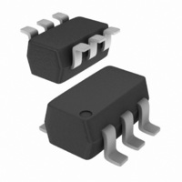
... NXP Semiconductors 10. Package outline Plastic surface-mounted package; 6 leads y 6 pin 1 index DIMENSIONS (mm are the original dimensions UNIT max 0.30 1.1 0.25 mm 0.1 0.20 0.8 0.10 OUTLINE VERSION IEC SOT363 Fig 33. Package outline SOT363 BF1210_1 Product data sheet scale 2.2 1.35 2.2 1 ...
Page 19
... NXP Semiconductors 11. Abbreviations Table 14. Acronym AGC DC MOSFET UHF VHF 12. Revision history Table 15. Revision history Document ID Release date BF1210_1 20061025 BF1210_1 Product data sheet Abbreviations Description Automatic Gain Control Direct Current Metal-Oxide-Semiconductor Field-Effect Transistor Ultra High Frequency Very High Frequency Data sheet status Product data sheet Rev. 01 — ...
Page 20
... For detailed and full information see the relevant full data sheet, which is available on request via the local NXP Semiconductors sales office. In case of any inconsistency or conflict with the short data sheet, the full data sheet shall prevail ...
Page 21
... NXP Semiconductors 15. Contents 1 Product profi 1.1 General description 1.2 Features . . . . . . . . . . . . . . . . . . . . . . . . . . . . . . 1 1.3 Applications . . . . . . . . . . . . . . . . . . . . . . . . . . . 1 1.4 Quick reference data Pinning information . . . . . . . . . . . . . . . . . . . . . . 2 3 Ordering information . . . . . . . . . . . . . . . . . . . . . 2 4 Marking . . . . . . . . . . . . . . . . . . . . . . . . . . . . . . . . 3 5 Limiting values Thermal characteristics Static characteristics Dynamic characteristics . . . . . . . . . . . . . . . . . . 4 8.1 Dynamic characteristics for amplifi 8.1.1 Graphs for amplifi 8.1.2 Scattering parameters for amplifi ...