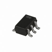
BF1102R,115 NXP Semiconductors, BF1102R,115 Datasheet

BF1102R,115
Specifications of BF1102R,115
Related parts for BF1102R,115
BF1102R,115 Summary of contents
Page 1
DATA SHEET dbook, halfpage BF1102; BF1102R Dual N-channel dual gate MOS-FETs Product specification Supersedes data of 1999 Jul 01 DISCRETE SEMICONDUCTORS MBD128 2000 Apr 11 ...
Page 2
... NXP Semiconductors Dual N-channel dual gate MOS-FETs FEATURES Two low noise gain controlled amplifiers in a single package Specially designed for 5 V applications Superior cross-modulation performance during AGC High forward transfer admittance High forward transfer admittance to input capacitance ratio ...
Page 3
... NXP Semiconductors Dual N-channel dual gate MOS-FETs LIMITING VALUES In accordance with the Absolute Maximum Rating System (IEC 60134). SYMBOL PARAMETER Per MOS-FET unless otherwise specified V drain-source voltage DS I drain current (DC gate 1 current G1 I gate 2 current G2 P total power dissipation tot T storage temperature ...
Page 4
... NXP Semiconductors Dual N-channel dual gate MOS-FETs STATIC CHARACTERISTICS = 25 C unless otherwise specified SYMBOL PARAMETER Per MOS-FET unless otherwise specified V drain-source breakdown voltage (BR)DSS V gate 1-source breakdown voltage V (BR)G1-SS V gate 2-source breakdown voltage V (BR)G2-SS V forward source-gate 1 voltage (F)S-G1 V forward source-gate 2 voltage ...
Page 5
... NXP Semiconductors Dual N-channel dual gate MOS-FETs ALL GRAPHS FOR ONE MOS-FET 30 handbook, halfpage (mA 0.4 0.8 1 Fig.3 Transfer characteristics; typical values. 160 handbook, halfpage V G2 (μA) 120 0 Fig.5 Gate 1 current as a function of gate 1 voltage; typical values. 2000 Apr 11 ...
Page 6
... NXP Semiconductors Dual N-channel dual gate MOS-FETs 25 handbook, halfpage I D (mA G2-S j Fig.7 Drain current as a function of gate 1 current; typical values. 30 handbook, halfpage kΩ (mA G2 connected see Fig.20 Fig.9 Drain current as a function of gate and drain supply voltage; typical values. 2000 Apr 11 ...
Page 7
... NXP Semiconductors Dual N-channel dual gate MOS-FETs 40 handbook, halfpage I G1 (μ 120 k (connected see Fig.20 Fig.11 Gate 1 current as a function of gate 2 voltage; typical values. 120 handbook, halfpage V unw (dB μV) 110 100 MHz unw R = 120 k (connected see Fig.20 Fig.13 Unwanted voltage for 1% cross-modulation as a function of gain reduction ...
Page 8
... NXP Semiconductors Dual N-channel dual gate MOS-FETs 2 10 handbook, halfpage y is (mS − mA amb Fig.15 Input admittance as a function of frequency; typical values handbook, halfpage | (mS mA amb Fig.17 Forward transfer admittance and phase as a function of frequency; typical values. 2000 Apr 11 MGS370 handbook, halfpage ...
Page 9
... NXP Semiconductors Dual N-channel dual gate MOS-FETs 0 handbook, halfpage crosstalk level (dB) −20 −40 −60 −80 0 200 400 Active amplifier Non-active amplifier G1-S Source and load impedances: 50 (both amplifiers C. T amb Fig.19 Crosstalk as a function of frequency: Output level of non-active amplifier related to output level of active amplifier ...
Page 10
... NXP Semiconductors Dual N-channel dual gate MOS-FETs Table 1 Scattering parameters MAGNITUDE ANGLE (MHz) (ratio) (deg) 5.6 50 0.987 11.1 100 0.981 21.9 200 0.961 32.1 300 0.933 42.0 400 0.899 51.1 500 0.867 59.9 600 0.834 67.9 700 0.805 75.7 800 0.779 ...
Page 11
... NXP Semiconductors Dual N-channel dual gate MOS-FETs PACKAGE OUTLINE Plastic surface-mounted package; 6 leads y 6 pin 1 index DIMENSIONS (mm are the original dimensions UNIT max 1.1 0.30 0.25 mm 0.1 0.20 0.8 0.10 OUTLINE VERSION IEC SOT363 2000 Apr scale 2.2 1.35 2.2 1.3 ...
Page 12
... In no event shall NXP Semiconductors be liable for any indirect, incidental, punitive, special or consequential damages (including - without limitation - lost profits, lost savings, business interruption, costs related to the ...
Page 13
... NXP Semiconductors’ specifications such use shall be solely at customer’s own risk, and (c) customer fully indemnifies NXP Semiconductors for any liability, damages or failed product claims resulting from customer design and use of the product for automotive applications beyond NXP Semiconductors’ ...
Page 14
... Interface, Security and Digital Processing expertise Customer notification This data sheet was changed to reflect the new company name NXP Semiconductors, including new legal definitions and disclaimers. No changes were made to the technical content, except for package outline drawings which were updated to the latest version. ...


