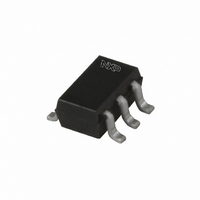
BF1102R,115 NXP Semiconductors, BF1102R,115 Datasheet - Page 4

BF1102R,115
Manufacturer Part Number
BF1102R,115
Description
MOSFET N-CH 7V 40MA SOT363R
Manufacturer
NXP Semiconductors
Datasheet
1.BF1102R115.pdf
(14 pages)
Specifications of BF1102R,115
Package / Case
SC-70-6, SC-88, SOT-363
Current Rating
40mA
Frequency
800MHz
Transistor Type
N-Channel Dual Gate
Noise Figure
2dB
Current - Test
15mA
Voltage - Test
5V
Configuration
Dual
Continuous Drain Current
0.04 A
Drain-source Breakdown Voltage
7 V
Gate-source Breakdown Voltage
+/- 6 V
Maximum Operating Temperature
+ 150 C
Minimum Operating Temperature
- 65 C
Mounting Style
SMD/SMT
Power Dissipation
200 mW
Transistor Polarity
N-Channel
Lead Free Status / RoHS Status
Lead free / RoHS Compliant
Power - Output
-
Gain
-
Lead Free Status / Rohs Status
Lead free / RoHS Compliant
Other names
934055823115::BF1102R T/R::BF1102R T/R
NXP Semiconductors
STATIC CHARACTERISTICS
T
Note
1. R
DYNAMIC CHARACTERISTICS
Common source; T
Notes
1. Not used MOS-FET: V
2. Gate 2 capacitance of both MOS-FETs.
3. Measured in test circuit of Fig.20.
2000 Apr 11
Per MOS-FET unless otherwise specified
V
V
V
V
V
V
V
I
I
I
Per MOS-FET unless otherwise specified (note 1)
y
C
C
C
C
F
X
j
SYMBOL
DSX
G1-S
G2-S
SYMBOL
= 25 C unless otherwise specified.
(BR)DSS
(BR)G1-SS
(BR)G2-SS
(F)S-G1
(F)S-G2
G1-S(th)
G2-S(th)
mod
Dual N-channel dual gate MOS-FETs
ig1-ss
ig2-ss
oss
rss
fs
G1
connects gate 1 to V
drain-source breakdown voltage
gate 1-source breakdown voltage V
gate 2-source breakdown voltage V
forward source-gate 1 voltage
forward source-gate 2 voltage
gate 1-source threshold voltage
gate 2-source threshold voltage
drain-source current
gate 1 cut-off current
gate 2 cut-off current
forward transfer admittance
input capacitance at gate 1
input capacitance at gate 2
output capacitance
reverse transfer capacitance
noise figure
cross-modulation
amb
PARAMETER
= 25 C; V
PARAMETER
G1-S
GG
= 0; V
= 5 V.
G2-S
DS
= 4 V; V
= 0.
T
f = 1 MHz
f = 1 MHz; (note 2)
f = 1 MHz
f = 1 MHz
f = 800 MHz; Y
f
DS
w
j
input level for k = 1% at 0 dB AGC
input level for k = 1% at 40 dB AGC
= 25 C
= 50 MHz; f
V
V
V
V
V
V
V
V
= 5 V; I
G1-S
GS
GS
G2-S
G1-S
DS
DS
G2-S
G1-S
G2-S
= 5 V; V
= 5 V; V
= V
= V
= V
= V
= V
= 4 V; V
= 5 V; V
= 5 V; V
D
DS
DS
= 15 mA; unless otherwise specified.
G2-S
DS
DS
CONDITIONS
4
unw
= 0; I
= 0; I
S
G2-S
G1-S
= 0; I
= 0; I
= Y
= 0; I
DS
G2-S
G1-S
= 60 MHz; (note 3)
CONDITIONS
G1-S
G2-S
S opt
= 4 V; I
= 4 V; I
= 5 V; R
S-G1
S-G2
= V
= V
D
= 10 mA
= 5 mA
= 10 A
= 10 mA
= 10 mA
DS
DS
D
D
G
= 0
= 0
= 100 A
= 100 A
= 120 k; note 1
36
2
85
100
BF1102; BF1102R
MIN.
7
6
6
0.5
0.5
0.3
0.3
12
43
2.8
1.6
30
2
MIN.
TYP.
Product specification
15
15
1.5
1.5
1
1.2
20
50
20
50
3.6
7
2.5
50
2.8
MAX.
MAX.
V
V
V
V
V
V
V
mA
nA
nA
mS
pF
pF
pF
fF
dB
dBV
dBV
UNIT
UNIT


