BLF4G10-160,112 NXP Semiconductors, BLF4G10-160,112 Datasheet - Page 9
BLF4G10-160,112
Manufacturer Part Number
BLF4G10-160,112
Description
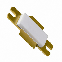
TRANSISTOR RF LDMOS SOT502A
Manufacturer
NXP Semiconductors
Specifications of BLF4G10-160,112
Package / Case
SOT502A
Transistor Type
LDMOS
Frequency
894MHz
Gain
19.7dB
Voltage - Rated
65V
Current Rating
15A
Current - Test
900mA
Voltage - Test
28V
Power - Output
160W
Configuration
Single
Transistor Polarity
N-Channel
Resistance Drain-source Rds (on)
0.065 Ohms
Drain-source Breakdown Voltage
65 V
Gate-source Breakdown Voltage
15 V
Continuous Drain Current
15 A
Maximum Operating Temperature
+ 200 C
Mounting Style
SMD/SMT
Minimum Operating Temperature
- 65 C
Lead Free Status / RoHS Status
Lead free / RoHS Compliant
Noise Figure
-
Lead Free Status / RoHS Status
Lead free / RoHS Compliant, Lead free / RoHS Compliant
Other names
934058737112
BLF4G10-160
BLF4G10-160
BLF4G10-160
BLF4G10-160


NXP Semiconductors
BLF4G10-160_1
Product data sheet
Fig 14. Circuit schematic for 869 MHz to 894 MHz CDMA demo test circuit
Fig 15. Component layout for 869 MHz to 894 MHz CDMA demo test circuit
L1
V
bias
See
The other side is unetched and serves as a ground plane.
See
(12 V - 28 V)
C1
Table 9
Table 9
C3
R10
R1
R2
R3
RF in
Q1
for a list of components
for a list of components.
R9
Q1
L2
C4
L1
V
bias
R4
Q2
R6
R5
C1
(12 V - 28 V)
R1
C3
R7
C4
R7
C5
L2
R6
R2
R4
R5
R8
C5
L3
R8
C6
R3
R10
L3
C7
C2
BLF4G10-160
R9
Q2
C6
L4
L5
CDMA in
Rev. 01 — 22 June 2007
C7
C2
L4
Q3
L5
Q3
BLF4G10-160
CDMA out
L6
L6
L7
L7
C8
C8
L8
UHF power LDMOS transistor
C9
C9 C10
L8
BLF4G10-160
C10
V
DD
V
(28 V)
L9
DD
C11
(28 V)
© NXP B.V. 2007. All rights reserved.
C12
L9
L10
C11
001aag559
RF out
001aag560
C12
L10
9 of 14
Related parts for BLF4G10-160,112
Image
Part Number
Description
Manufacturer
Datasheet
Request
R

Part Number:
Description:
RF MOSFET Small Signal LDMOS TNS
Manufacturer:
NXP Semiconductors
Datasheet:
Part Number:
Description:
Uhf Power Ldmos Transistor
Manufacturer:
NXP Semiconductors
Datasheet:
Part Number:
Description:
NXP Semiconductors designed the LPC2420/2460 microcontroller around a 16-bit/32-bitARM7TDMI-S CPU core with real-time debug interfaces that include both JTAG andembedded trace
Manufacturer:
NXP Semiconductors
Datasheet:

Part Number:
Description:
NXP Semiconductors designed the LPC2458 microcontroller around a 16-bit/32-bitARM7TDMI-S CPU core with real-time debug interfaces that include both JTAG andembedded trace
Manufacturer:
NXP Semiconductors
Datasheet:
Part Number:
Description:
NXP Semiconductors designed the LPC2468 microcontroller around a 16-bit/32-bitARM7TDMI-S CPU core with real-time debug interfaces that include both JTAG andembedded trace
Manufacturer:
NXP Semiconductors
Datasheet:
Part Number:
Description:
NXP Semiconductors designed the LPC2470 microcontroller, powered by theARM7TDMI-S core, to be a highly integrated microcontroller for a wide range ofapplications that require advanced communications and high quality graphic displays
Manufacturer:
NXP Semiconductors
Datasheet:
Part Number:
Description:
NXP Semiconductors designed the LPC2478 microcontroller, powered by theARM7TDMI-S core, to be a highly integrated microcontroller for a wide range ofapplications that require advanced communications and high quality graphic displays
Manufacturer:
NXP Semiconductors
Datasheet:
Part Number:
Description:
The Philips Semiconductors XA (eXtended Architecture) family of 16-bit single-chip microcontrollers is powerful enough to easily handle the requirements of high performance embedded applications, yet inexpensive enough to compete in the market for hi
Manufacturer:
NXP Semiconductors
Datasheet:
Part Number:
Description:
The XA-S3 device is a member of Philips Semiconductors? XA(eXtended Architecture) family of high performance 16-bitsingle-chip microcontrollers
Manufacturer:
NXP Semiconductors
Datasheet:

Part Number:
Description:
The NXP BlueStreak LH75401/LH75411 family consists of two low-cost 16/32-bit System-on-Chip (SoC) devices
Manufacturer:
NXP Semiconductors
Datasheet:
Part Number:
Description:
The NXP LPC3130/3131 combine an 180 MHz ARM926EJ-S CPU core, high-speed USB2
Manufacturer:
NXP Semiconductors
Datasheet:
Part Number:
Description:
The NXP LPC3141 combine a 270 MHz ARM926EJ-S CPU core, High-speed USB 2
Manufacturer:
NXP Semiconductors
Part Number:
Description:
The NXP LPC3143 combine a 270 MHz ARM926EJ-S CPU core, High-speed USB 2
Manufacturer:
NXP Semiconductors

Part Number:
Description:
The NXP LPC3152 combines an 180 MHz ARM926EJ-S CPU core, High-speed USB 2
Manufacturer:
NXP Semiconductors