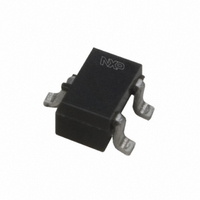
BFS505,115 NXP Semiconductors, BFS505,115 Datasheet - Page 2

BFS505,115
Manufacturer Part Number
BFS505,115
Description
TRANS NPN 15V 9GHZ SOT323
Manufacturer
NXP Semiconductors
Datasheet
1.BFS505115.pdf
(14 pages)
Specifications of BFS505,115
Package / Case
SC-70-3, SOT-323-3
Transistor Type
NPN
Voltage - Collector Emitter Breakdown (max)
15V
Frequency - Transition
9GHz
Noise Figure (db Typ @ F)
1.2dB ~ 2.1dB @ 900MHz
Power - Max
150mW
Dc Current Gain (hfe) (min) @ Ic, Vce
60 @ 5mA, 6V
Current - Collector (ic) (max)
18mA
Mounting Type
Surface Mount
Dc Current Gain Hfe Max
60 @ 5mA @ 6V
Mounting Style
SMD/SMT
Configuration
Single
Transistor Polarity
NPN
Maximum Operating Frequency
9000 MHz (Typ)
Collector- Emitter Voltage Vceo Max
15 V
Emitter- Base Voltage Vebo
2.5 V
Continuous Collector Current
0.018 A
Power Dissipation
150 mW
Maximum Operating Temperature
+ 175 C
Lead Free Status / RoHS Status
Lead free / RoHS Compliant
Gain
-
Lead Free Status / Rohs Status
Lead free / RoHS Compliant
Other names
568-1991-2
934021370115
BFS505 T/R
934021370115
BFS505 T/R
Available stocks
Company
Part Number
Manufacturer
Quantity
Price
Part Number:
BFS505,115
Manufacturer:
NXP/恩智浦
Quantity:
20 000
NXP Semiconductors
FEATURES
Low current consumption
High power gain
Low noise figure
High transition frequency
Gold metallization ensures
SOT323 envelope.
DESCRIPTION
NPN transistor in a plastic SOT323
envelope.
It is intended for low power amplifiers,
oscillators and mixers particularly in
RF portable communication
equipment (cellular phones, cordless
phones, pagers) up to 2 GHz.
QUICK REFERENCE DATA
Note
1. T
September 1995
V
V
I
P
h
f
G
F
SYMBOL
C
T
FE
excellent reliability
CBO
CES
tot
NPN 9 GHz wideband transistor
UM
s
is the temperature at the soldering point of the collector tab.
collector-base voltage
collector-emitter voltage
DC collector current
total power dissipation
DC current gain
transition frequency
maximum unilateral power gain
noise figure
PARAMETER
PINNING
PIN
1
2
3
open emitter
R
up to T
I
I
T
I
T
I
f = 900 MHz; T
base
emitter
collector
C
C
c
c
amb
amb
BE
= 5 mA; V
= 1.25 mA; V
= 5 mA; V
= 5 mA; V
= 0
Code: N0
= 25 C
= 25 C
DESCRIPTION
s
= 147 C; note 1
2
CONDITIONS
CE
CE
CE
amb
= 6 V; f = 900 MHz;
CE
= 6 V; T
= 6 V; f = 1 GHz;
= 6 V;
= 25 C
j
= 25 C
handbook, 2 columns
60
MIN.
Top view
Fig.1 SOT323.
120
9
17
1.2
Product specification
TYP.
1
3
BFS505
20
15
18
150
250
1.7
MBC870
MAX.
2
V
V
mA
mW
GHz
dB
dB
UNIT


