BFG21W,115 NXP Semiconductors, BFG21W,115 Datasheet - Page 2
BFG21W,115
Manufacturer Part Number
BFG21W,115
Description
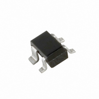
TRANS NPN 15V .5A 18GHZ CMPAK-4
Manufacturer
NXP Semiconductors
Datasheet
1.BFG21W115.pdf
(11 pages)
Specifications of BFG21W,115
Package / Case
CMPAK-4
Transistor Type
NPN
Voltage - Collector Emitter Breakdown (max)
4.5V
Frequency - Transition
18GHz
Power - Max
600mW
Dc Current Gain (hfe) (min) @ Ic, Vce
40 @ 200mA, 2V
Current - Collector (ic) (max)
500mA
Mounting Type
Surface Mount
Dc Current Gain Hfe Max
40 @ 200mA @ 2V
Mounting Style
SMD/SMT
Configuration
Single Dual Emitter
Transistor Polarity
NPN
Maximum Operating Frequency
18000 MHz (Min)
Collector- Emitter Voltage Vceo Max
4.5 V
Emitter- Base Voltage Vebo
1 V
Continuous Collector Current
0.5 A
Power Dissipation
600 mW
Maximum Operating Temperature
+ 150 C
Lead Free Status / RoHS Status
Lead free / RoHS Compliant
Gain
-
Noise Figure (db Typ @ F)
-
Lead Free Status / Rohs Status
Lead free / RoHS Compliant
Other names
568-1974-2
934047480115
BFG21W T/R
934047480115
BFG21W T/R


NXP Semiconductors
FEATURES
High power gain
High efficiency
1.9 GHz operating area
Linear and non-linear operation.
APPLICATIONS
Common emitter class-AB output stage in hand held
Driver for DCS1800, 1900.
DESCRIPTION
NPN double polysilicon bipolar power transistor with
buried layer for low voltage medium power applications
encapsulated in a plastic, 4-pin dual-emitter SOT343R
package.
QUICK REFERENCE DATA
RF performance at T
1998 Jul 06
Pulsed class-AB; < 1 : 2; t
radio equipment at 1.9 GHz such as DECT, PHS, etc.
UHF power transistor
MODE OF OPERATION
s
60 C in a common emitter test circuit.
p
= 5 ms
(GHz)
1.9
f
2
PINNING
handbook, halfpage
Marking code: P1.
V
3.6
(V)
CE
Fig.1 Simplified outline SOT343R.
PIN
1, 3
2
4
(dBm)
P
26
3
2
Top view
L
emitter
base
collector
MSB842
4
1
(dB)
10
G
Product specification
DESCRIPTION
p
BFG21W
typ.55
(%)
C
Related parts for BFG21W,115
Image
Part Number
Description
Manufacturer
Datasheet
Request
R

Part Number:
Description:
NXP Semiconductors designed the LPC2420/2460 microcontroller around a 16-bit/32-bitARM7TDMI-S CPU core with real-time debug interfaces that include both JTAG andembedded trace
Manufacturer:
NXP Semiconductors
Datasheet:

Part Number:
Description:
NXP Semiconductors designed the LPC2458 microcontroller around a 16-bit/32-bitARM7TDMI-S CPU core with real-time debug interfaces that include both JTAG andembedded trace
Manufacturer:
NXP Semiconductors
Datasheet:
Part Number:
Description:
NXP Semiconductors designed the LPC2468 microcontroller around a 16-bit/32-bitARM7TDMI-S CPU core with real-time debug interfaces that include both JTAG andembedded trace
Manufacturer:
NXP Semiconductors
Datasheet:
Part Number:
Description:
NXP Semiconductors designed the LPC2470 microcontroller, powered by theARM7TDMI-S core, to be a highly integrated microcontroller for a wide range ofapplications that require advanced communications and high quality graphic displays
Manufacturer:
NXP Semiconductors
Datasheet:
Part Number:
Description:
NXP Semiconductors designed the LPC2478 microcontroller, powered by theARM7TDMI-S core, to be a highly integrated microcontroller for a wide range ofapplications that require advanced communications and high quality graphic displays
Manufacturer:
NXP Semiconductors
Datasheet:
Part Number:
Description:
The Philips Semiconductors XA (eXtended Architecture) family of 16-bit single-chip microcontrollers is powerful enough to easily handle the requirements of high performance embedded applications, yet inexpensive enough to compete in the market for hi
Manufacturer:
NXP Semiconductors
Datasheet:
Part Number:
Description:
The XA-S3 device is a member of Philips Semiconductors? XA(eXtended Architecture) family of high performance 16-bitsingle-chip microcontrollers
Manufacturer:
NXP Semiconductors
Datasheet:

Part Number:
Description:
The NXP BlueStreak LH75401/LH75411 family consists of two low-cost 16/32-bit System-on-Chip (SoC) devices
Manufacturer:
NXP Semiconductors
Datasheet:
Part Number:
Description:
The NXP LPC3130/3131 combine an 180 MHz ARM926EJ-S CPU core, high-speed USB2
Manufacturer:
NXP Semiconductors
Datasheet:
Part Number:
Description:
The NXP LPC3141 combine a 270 MHz ARM926EJ-S CPU core, High-speed USB 2
Manufacturer:
NXP Semiconductors
Part Number:
Description:
The NXP LPC3143 combine a 270 MHz ARM926EJ-S CPU core, High-speed USB 2
Manufacturer:
NXP Semiconductors

Part Number:
Description:
The NXP LPC3152 combines an 180 MHz ARM926EJ-S CPU core, High-speed USB 2
Manufacturer:
NXP Semiconductors
Part Number:
Description:
The NXP LPC3154 combines an 180 MHz ARM926EJ-S CPU core, High-speed USB 2
Manufacturer:
NXP Semiconductors

Part Number:
Description:
Standard level N-channel enhancement mode Field-Effect Transistor (FET) in a plastic package using NXP High-Performance Automotive (HPA) TrenchMOS technology
Manufacturer:
NXP Semiconductors
Datasheet: