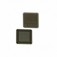
SI5326C-C-GM Silicon Laboratories Inc, SI5326C-C-GM Datasheet - Page 18

SI5326C-C-GM
Manufacturer Part Number
SI5326C-C-GM
Description
DSPLL 36-Pin QFN EP
Manufacturer
Silicon Laboratories Inc
Type
Jitter Attenuatorr
Datasheet
1.SI5326B-C-GM.pdf
(72 pages)
Specifications of SI5326C-C-GM
Package
36QFN EP
Operating Temperature
-40 to 85 °C
Pll
Yes
Input
Clock
Output
CML, CMOS, LVDS, LVPECL
Number Of Circuits
1
Ratio - Input:output
2:2
Differential - Input:output
Yes/Yes
Frequency - Max
346MHz
Divider/multiplier
Yes/Yes
Voltage - Supply
1.71 V ~ 3.63 V
Mounting Type
Surface Mount
Package / Case
36-QFN
Frequency-max
346MHz
Operating Temperature (max)
85C
Operating Temperature (min)
-40C
Package Type
QFN EP
Mounting
Surface Mount
Lead Free Status / RoHS Status
Lead free / RoHS Compliant
Lead Free Status / RoHS Status
Lead free / RoHS Compliant
Other names
336-1746
336-1746-5
336-1746
336-1746-5
336-1746
Available stocks
Company
Part Number
Manufacturer
Quantity
Price
Part Number:
SI5326C-C-GM
Manufacturer:
SILICON LABS/芯科
Quantity:
20 000
Si5326
4. Functional Description
The Si5326 is a jitter-attenuating precision clock
multiplier for applications requiring sub 1 ps jitter
performance. The Si5326 accepts two input clocks
ranging from 2 kHz to 710 MHz and generates two
output clocks ranging from 2 kHz to 945 MHz and select
frequencies to 1.4 GHz. The Si5326 can also use its
crystal oscillator as a clock source for frequency
synthesis. The device provides virtually any frequency
translation combination across this operating range.
Independent dividers are available for each input clock
and output clock, so the Si5326 can accept input clocks
at different frequencies and it can generate output
clocks at different frequencies. The Si5326 input clock
frequency
programmable through an I
Laboratories
DSPLLsim, that can be used to determine the optimum
PLL divider settings for a given input frequency/clock
multiplication ratio combination that minimizes phase
noise and power consumption. This utility can be
downloaded from http://www.silabs.com/timing.
The Si5326 is based on Silicon Laboratories' 3rd-
generation DSPLL
frequency synthesis and jitter attenuation in a highly
integrated PLL solution that eliminates the need for
external VCXO and loop filter components. The Si5326
PLL loop bandwidth is digitally programmable and
supports a range from 60 Hz to 8.4 kHz. The DSPLLsim
software utility can be used to calculate valid loop
bandwidth
frequency/clock multiplication ratio.
18
Frequency Offset
Loss of Signal/
Loss of Lock
CKIN1
CKIN2
and
settings
offers
®
clock
Xtal/Refclock
technology, which provides any
a
÷ N31
÷ N32
for
PC-based
Signal Detect
2
multiplication
C or SPI interface. Silicon
a
given
Hitless Switching
Device Interrupt
Figure 6. Functional Block Diagram
software
Xtal or Refclock
I
Mux
Rate Select
2
C/SPI Port
input
ratio
utility,
clock
are
Rev. 1.0
Control
DSPLL
÷ N2
The Si5326 supports hitless switching between the two
synchronous input clocks in compliance with GR-253-
CORE that greatly minimizes the propagation of phase
transients to the clock outputs during an input clock
transition (maximum 200 ps phase change). Manual
and automatic revertive and non-revertive input clock
switching options are available. The Si5326 monitors
both input clocks for loss-of-signal (LOS) and provides a
LOS alarm (INT_C1B and C2B) when it detects missing
pulses on either input clock. The device monitors the
lock status of the PLL. The lock detect algorithm works
by continuously monitoring the phase of the input clock
in relation to the phase of the feedback clock. The
Si5326 also monitors frequency offset alarms (FOS),
which indicate if an input clock is within a specified
frequency band relative to the frequency of a reference
clock. Both Stratum 3/3E and SONET Minimum Clock
(SMC) FOS thresholds are supported.The Si5326
provides a digital hold capability that allows the device
to continue generation of a stable output clock when the
selected input reference is lost. During digital hold, the
DSPLL generates an output frequency based on a
historical average frequency that existed for a fixed
amount of time before the error event occurred,
eliminating the effects of phase and frequency
transients that may occur immediately preceding digital
hold.
®
Skew Control
Clock Select
÷ N1_HS
÷ N1_LS
÷ N2_LS
GND
VDD (1.8, 2.5, or 3.3 V)
CKOUT1
CKOUT2


