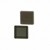
SI5326C-C-GM Silicon Laboratories Inc, SI5326C-C-GM Datasheet - Page 26

SI5326C-C-GM
Manufacturer Part Number
SI5326C-C-GM
Description
DSPLL 36-Pin QFN EP
Manufacturer
Silicon Laboratories Inc
Type
Jitter Attenuatorr
Datasheet
1.SI5326B-C-GM.pdf
(72 pages)
Specifications of SI5326C-C-GM
Package
36QFN EP
Operating Temperature
-40 to 85 °C
Pll
Yes
Input
Clock
Output
CML, CMOS, LVDS, LVPECL
Number Of Circuits
1
Ratio - Input:output
2:2
Differential - Input:output
Yes/Yes
Frequency - Max
346MHz
Divider/multiplier
Yes/Yes
Voltage - Supply
1.71 V ~ 3.63 V
Mounting Type
Surface Mount
Package / Case
36-QFN
Frequency-max
346MHz
Operating Temperature (max)
85C
Operating Temperature (min)
-40C
Package Type
QFN EP
Mounting
Surface Mount
Lead Free Status / RoHS Status
Lead free / RoHS Compliant
Lead Free Status / RoHS Status
Lead free / RoHS Compliant
Other names
336-1746
336-1746-5
336-1746
336-1746-5
336-1746
Available stocks
Company
Part Number
Manufacturer
Quantity
Price
Part Number:
SI5326C-C-GM
Manufacturer:
SILICON LABS/芯科
Quantity:
20 000
Si5326
Reset value = 0010 1101
26
Register 6.
Name
Type
5:3
2:0
Bit
Bit
7
6
Reserved
SFOUT2_
SFOUT1_
REG [2:0]
REG [2:0]
Reserved
SLEEP
Name
D7
R
SLEEP
Reserved.
SLEEP.
In sleep mode, all clock outputs are disabled and the maximum amount of internal cir-
cuitry is powered down to reduce power dissipation and noise generation. This bit over-
rides the SFOUTn_REG[2:0] output signal format settings.
0: Normal operation
1: Sleep mode
SFOUT2_REG [2:0].
Controls output signal format and disable for CKOUT2 output buffer.
000: Reserved
001: Disable
010: CMOS (Bypass mode not supported)
011: Low swing LVDS
100: Reserved
101: LVPECL
110: CML
111: LVDS
Note: LVPECL requires a nominal V
SFOUT1_REG [2:0].
Controls output signal format and disable for CKOUT1 output buffer.
000: Reserved
001: Disable
010: CMOS (Bypass mode not supported)
011: Low swing LVDS
100: Reserved
101: LVPECL
110: CML
111: LVDS
Note: LVPECL requires a nominal V
R/W
D6
D5
SFOUT2_REG [2:0]
R/W
Rev. 1.0
D4
DD
DD
2.5 V.
2.5 V.
Function
D3
D2
SFOUT1_REG [2:0]
R/W
D1
D0


