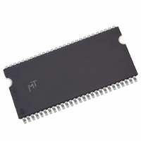
MT48LC16M16A2P-7E IT:D Micron Technology Inc, MT48LC16M16A2P-7E IT:D Datasheet - Page 32

MT48LC16M16A2P-7E IT:D
Manufacturer Part Number
MT48LC16M16A2P-7E IT:D
Description
DRAM Chip SDRAM 256M-Bit 16Mx16 3.3V 54-Pin TSOP-II Tray
Manufacturer
Micron Technology Inc
Type
SDRAMr
Specifications of MT48LC16M16A2P-7E IT:D
Density
256 Mb
Maximum Clock Rate
143 MHz
Package
54TSOP-II
Address Bus Width
15 Bit
Operating Supply Voltage
3.3 V
Maximum Random Access Time
5.4 ns
Operating Temperature
-40 to 85 °C
Format - Memory
RAM
Memory Type
SDRAM
Memory Size
256M (16Mx16)
Speed
133MHz
Interface
Parallel
Voltage - Supply
3 V ~ 3.6 V
Package / Case
54-TSOP II
Organization
16Mx16
Address Bus
15b
Access Time (max)
5.4ns
Operating Supply Voltage (typ)
3.3V
Package Type
TSOP-II
Operating Temp Range
-40C to 85C
Operating Supply Voltage (max)
3.6V
Operating Supply Voltage (min)
3V
Supply Current
135mA
Pin Count
54
Mounting
Surface Mount
Operating Temperature Classification
Industrial
Lead Free Status / RoHS Status
Lead free / RoHS Compliant
Commands
Table 16: Truth Table – Commands and DQM Operation
Note 1 applies to all parameters and conditions
COMMAND INHIBIT
PDF: 09005aef8091e6d1
256Mb_sdr.pdf - Rev. N 1/10 EN
Name (Function)
COMMAND INHIBIT (NOP)
NO OPERATION (NOP)
ACTIVE (select bank and activate row)
READ (select bank and column, and start READ burst)
WRITE (select bank and column, and start WRITE burst)
BURST TERMINATE
PRECHARGE (Deactivate row in bank or banks)
AUTO REFRESH or SELF REFRESH (enter self refresh mode)
LOAD MODE REGISTER
Write enable/output enable
Write inhibit/output High-Z
Notes:
The following table provides a quick reference of available commands, followed by a
written description of each command. Additional Truth Tables (Table 17 (page 38),
Table 18 (page 40), and Table 19 (page 42)) provide current state/next state informa-
tion.
The COMMAND INHIBIT function prevents new commands from being executed by
the device, regardless of whether the CLK signal is enabled. The device is effectively de-
selected. Operations already in progress are not affected.
1. CKE is HIGH for all commands shown except SELF REFRESH.
2. A[0:n] provide row address (where An is the most significant address bit), BA0 and BA1
3. A[0:i] provide column address (where i = the most significant column address for a given
4. The purpose of the BURST TERMINATE command is to stop a data burst, thus the com-
5. A10 LOW: BA0, BA1 determine the bank being precharged. A10 HIGH: all banks pre-
6. This command is AUTO REFRESH if CKE is HIGH, SELF REFRESH if CKE is LOW.
7. Internal refresh counter controls row addressing; all inputs and I/Os are “Don’t Care”
8. A[11:0] define the op-code written to the mode register.
9. Activates or deactivates the DQ during WRITEs (zero-clock delay) and READs (two-clock
determine which bank is made active.
device configuration). A10 HIGH enables the auto precharge feature (nonpersistent),
while A10 LOW disables the auto precharge feature. BA0 and BA1 determine which
bank is being read from or written to.
mand could coincide with data on the bus. However, the DQ column reads a “Don’t
Care” state to illustrate that the BURST TERMINATE command can occur when there is
no data present.
charged and BA0, BA1 are “Don’t Care.”
except for CKE.
delay).
32
CS# RAS# CAS# WE# DQM
H
X
X
L
L
L
L
L
L
L
L
H
H
H
H
Micron Technology, Inc. reserves the right to change products or specifications without notice.
X
X
X
L
L
L
L
X
H
H
H
H
X
X
L
L
L
L
256Mb: x4, x8, x16 SDRAM
H
H
H
H
X
X
X
L
L
L
L
L/H
L/H
X
X
X
X
X
X
X
H
L
© 1999 Micron Technology, Inc. All rights reserved.
Bank/row
Bank/col
Bank/col
Op-code
ADDR
Code
X
X
X
X
X
X
Commands
High-Z
Active
Active
Valid
DQ
X
X
X
X
X
X
X
Notes
6, 7
2
3
3
4
5
8
9
9


