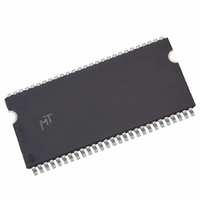
MT48LC16M16A2P-7E IT:D Micron Technology Inc, MT48LC16M16A2P-7E IT:D Datasheet - Page 91

MT48LC16M16A2P-7E IT:D
Manufacturer Part Number
MT48LC16M16A2P-7E IT:D
Description
DRAM Chip SDRAM 256M-Bit 16Mx16 3.3V 54-Pin TSOP-II Tray
Manufacturer
Micron Technology Inc
Type
SDRAMr
Specifications of MT48LC16M16A2P-7E IT:D
Density
256 Mb
Maximum Clock Rate
143 MHz
Package
54TSOP-II
Address Bus Width
15 Bit
Operating Supply Voltage
3.3 V
Maximum Random Access Time
5.4 ns
Operating Temperature
-40 to 85 °C
Format - Memory
RAM
Memory Type
SDRAM
Memory Size
256M (16Mx16)
Speed
133MHz
Interface
Parallel
Voltage - Supply
3 V ~ 3.6 V
Package / Case
54-TSOP II
Organization
16Mx16
Address Bus
15b
Access Time (max)
5.4ns
Operating Supply Voltage (typ)
3.3V
Package Type
TSOP-II
Operating Temp Range
-40C to 85C
Operating Supply Voltage (max)
3.6V
Operating Supply Voltage (min)
3V
Supply Current
135mA
Pin Count
54
Mounting
Surface Mount
Operating Temperature Classification
Industrial
Lead Free Status / RoHS Status
Lead free / RoHS Compliant
Rev. E – 3/02
Rev. D – 7/01
Rev. C – 3/01
PDF: 09005aef8091e6d1
256Mb_sdr.pdf - Rev. N 1/10 EN
• Added 54-ball FBGA package information to front page.
• Added 54-ball FBGA pinout drawing to then-page 3.
• Added 54-ball FBGA package part numbers to then-page 4.
• Added 54-ball FBGA pin descriptions to then-page 10.
• Updated DQM information in 60-ball FGBA pin descriptions on then-page 11.
• Added 54-ball FGBA mech drawing to then-page 59.
• Removed Preliminary status.
• Updated x4 and x8 FBGA row label from Q to R on then-page 2.
• Moved "(to state (A10 LOW})" on then-page 8.
• Updated I
• Added Capacitance table for FBGA to then-page 34.
• Added notes 34-36 for FBGA capacitance (MIN) values different from PC133 on then-
• Changed note 9 and 11 V
• Corrected Initialization waveform (
• Added "FB" FBGA package for x4- and x8-only configurations on then-pages 1 and 3.
• Added new page with FBGA pinout for x4 and x8 configurations on then-page 2.
• Removed -8E speed grade reference on then-pages 1, 11, and 33-55.
• Updated
• Updated Mode Register for A12 from unused to reserved on then-page 10.
• Changed
• Updated MAX -7E/ -75 I
• Added reference "notes appear on page 36" on then-pages 33-35.
• Removed temp reference and added note 5 to all tables.
• Note 21 updated for
• Updated "Don't Care" state of the SELF REFRESH MODE diagram on then-page 41.
• Updated A0-A11 to A0-A9, A11 as A10 is isolated for AP.
• Updated Single READ w/o AP to include note 3 at T3 and T4 NOP cmds on then-page
• Updated Write w/o AP to show
page 36.
1.4V reference level.
44.
page 49.
– I
– I
– I
– I
– I
– I
– I
DD1
DD3
DD4
DD5
DD6
DD7
DD7
t
from 170/160 to 130/120 for -7E/-75.
from 60/60 to 45/40 for -7E/-75.
from 160/160 to 130/130 for -7E/-75.
from 340/320 to 285/270 for -7E/-75.
from 4/4 to 3.5/3.5 for -7E/-75.
from 3/3 to 2.5/2.5 for -7E/-75.
(low power) from 2/2 to 1.5/1.5 for -7E/-75.
t
OH(MIN) value from 2.7ns to 3ns on then-pages 34, 39, 42-48.
DD
RC to
(MAX) Specifications to reflect 71G power edits on then-page 33:
t
RFC for burst AUTO REFRESH commands on then-page 14.
t
CK=ns units vs. MHz reference.
DD5
IH(MIN)
91
from 300/300 to 340/320 respectively on then-page 33.
t
-V
WR = 2 clks and updated note 2 to <Dinm+3> on then-
IL (MAX)
t
CMS and
Micron Technology, Inc. reserves the right to change products or specifications without notice.
test conditions from 0V-3V to 0.8V- 2.0V with
t
CMH reversed) on then-page 37.
256Mb: x4, x8, x16 SDRAM
© 1999 Micron Technology, Inc. All rights reserved.
Revision History


