MT48LC4M32LFF5-8 IT:G TR Micron Technology Inc, MT48LC4M32LFF5-8 IT:G TR Datasheet - Page 17
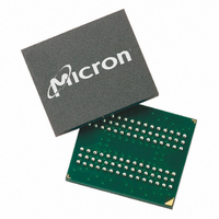
MT48LC4M32LFF5-8 IT:G TR
Manufacturer Part Number
MT48LC4M32LFF5-8 IT:G TR
Description
DRAM Chip Mobile SDRAM 128M-Bit 4Mx32 3.3V 90-Pin VFBGA T/R
Manufacturer
Micron Technology Inc
Type
Mobile SDRAMr
Datasheet
1.MT48LC8M16LFB4-75MG_TR.pdf
(80 pages)
Specifications of MT48LC4M32LFF5-8 IT:G TR
Density
128 Mb
Maximum Clock Rate
125 MHz
Package
90VFBGA
Address Bus Width
14 Bit
Operating Supply Voltage
3.3 V
Maximum Random Access Time
19|8|7 ns
Operating Temperature
-40 to 85 °C
Format - Memory
RAM
Memory Type
Mobile SDRAM
Memory Size
128M (4Mx32)
Speed
125MHz
Interface
Parallel
Voltage - Supply
3 V ~ 3.6 V
Package / Case
90-VFBGA
Organization
4Mx32
Address Bus
14b
Access Time (max)
19/8/7ns
Operating Supply Voltage (typ)
3.3V
Package Type
VFBGA
Operating Temp Range
-40C to 85C
Operating Supply Voltage (max)
3.6V
Operating Supply Voltage (min)
3V
Supply Current
115mA
Pin Count
90
Mounting
Surface Mount
Operating Temperature Classification
Industrial
Lead Free Status / RoHS Status
Contains lead / RoHS non-compliant


Burst Length (BL)
Burst Type
PDF: 09005aef807f4885/Source: 09005aef8071a76b
128Mbx16x32Mobile_2.fm - Rev. M 1/09 EN
The mode register must be loaded when all banks are idle, and the controller must wait
the specified time before initiating the subsequent operation. Violating either of these
requirements will result in unspecified operation.
Read and write accesses to the SDRAM are burst oriented, with BL being programmable,
as shown in Figure 8 on page 20. BL determines the maximum number of column loca-
tions that can be accessed for a given READ or WRITE command. Burst lengths of 1, 2, 4,
or 8 locations are available for both the sequential and the interleaved burst types, and a
full-page burst is available for the sequential mode. The full-page burst is used in
conjunction with the BURST TERMINATE command to generate arbitrary burst lengths.
If a full page burst is not terminated at the end of the page, it could wrap to column zero
and continue.
Reserved states cannot be used because unknown operation or incompatibility with
future versions may result.
When a READ or WRITE command is issued, a block of columns equal to BL is effectively
selected. All accesses for that burst take place within this block, meaning that the burst
will wrap within the block if a boundary is reached. The block is uniquely selected by A1–
A8 (x16) or A1–A7 (x32) when BL = 2; by A2–A8 (x16) or A2–A7 (x32) when BL = 4; and by
A3–A8 (x16) or A3–A7 (x32) when BL = 8. The remaining (least significant) address bit(s)
is (are) used to select the starting location within the block. Full-page bursts wrap within
the page if the boundary is reached.
Accesses within a given burst may be programmed either to be sequential or interleaved;
this is referred to as the burst type and is selected via bit M3. Note only a sequential burst
is allowed for full page bursts.
The ordering of accesses within a burst is determined by BL, the burst type, and the
starting column address, as shown in Table 6 on page 19.
17
Micron Technology, Inc., reserves the right to change products or specifications without notice.
128Mb: x16, x32 Mobile SDRAM
©2001 Micron Technology, Inc. All rights reserved.
Register Definition
Related parts for MT48LC4M32LFF5-8 IT:G TR
Image
Part Number
Description
Manufacturer
Datasheet
Request
R

Part Number:
Description:
IC SDRAM 128MBIT 125MHZ 90VFBGA
Manufacturer:
Micron Technology Inc
Datasheet:
Part Number:
Description:
IC SDRAM 128MBIT 125MHZ 90VFBGA
Manufacturer:
Micron Technology Inc
Datasheet:
Part Number:
Description:
IC SDRAM 128MBIT 100MHZ 90VFBGA
Manufacturer:
Micron Technology Inc
Datasheet:
Part Number:
Description:
IC SDRAM 128MBIT 100MHZ 90VFBGA
Manufacturer:
Micron Technology Inc
Datasheet:
Part Number:
Description:
DRAM Chip Mobile SDRAM 128M-Bit 4Mx32 3.3V 90-Pin VFBGA Tray
Manufacturer:
Micron Technology Inc
Datasheet:

Part Number:
Description:
Manufacturer:
Micron Technology Inc
Datasheet:

Part Number:
Description:
IC SDRAM 64MBIT 133MHZ 54TSOP
Manufacturer:
Micron Technology Inc
Datasheet:

Part Number:
Description:
IC SDRAM 64MBIT 5.5NS 86TSOP
Manufacturer:
Micron Technology Inc
Datasheet:
Part Number:
Description:
IC SDRAM 64MBIT 200MHZ 86TSOP
Manufacturer:
Micron Technology Inc
Datasheet:
Part Number:
Description:
IC SDRAM 64MBIT 133MHZ 54TSOP
Manufacturer:
Micron Technology Inc
Datasheet:
Part Number:
Description:
IC SDRAM 128MBIT 133MHZ 54TSOP
Manufacturer:
Micron Technology Inc
Datasheet:

Part Number:
Description:
IC SDRAM 256MBIT 133MHZ 90VFBGA
Manufacturer:
Micron Technology Inc
Datasheet:
Part Number:
Description:
IC SDRAM 128MBIT 133MHZ 54TSOP
Manufacturer:
Micron Technology Inc
Datasheet:
Part Number:
Description:
IC SDRAM 256MBIT 133MHZ 54TSOP
Manufacturer:
Micron Technology Inc
Datasheet:

Part Number:
Description:
IC DDR SDRAM 512MBIT 6NS 66TSOP
Manufacturer:
Micron Technology Inc
Datasheet: