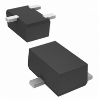
PBRN113EK,115 NXP Semiconductors, PBRN113EK,115 Datasheet - Page 4

PBRN113EK,115
Manufacturer Part Number
PBRN113EK,115
Description
TRANS NPN W/RES 40V SC-59A
Manufacturer
NXP Semiconductors
Datasheet
1.PBRN113ET215.pdf
(17 pages)
Specifications of PBRN113EK,115
Transistor Type
NPN - Pre-Biased
Current - Collector (ic) (max)
600mA
Voltage - Collector Emitter Breakdown (max)
40V
Resistor - Base (r1) (ohms)
1K
Resistor - Emitter Base (r2) (ohms)
1K
Dc Current Gain (hfe) (min) @ Ic, Vce
180 @ 300mA, 5V
Vce Saturation (max) @ Ib, Ic
1.15V @ 8mA, 800mA
Current - Collector Cutoff (max)
500nA
Power - Max
250mW
Mounting Type
Surface Mount
Package / Case
SC-59-3, SMT3, SOT-346, TO-236
Lead Free Status / RoHS Status
Lead free / RoHS Compliant
Other names
934058955115
PBRN113EK T/R
PBRN113EK T/R
PBRN113EK T/R
PBRN113EK T/R
NXP Semiconductors
PBRN113E_SER_1
Product data sheet
Table 6.
In accordance with the Absolute Maximum Rating System (IEC 60134).
[1]
[2]
[3]
Symbol
P
T
T
T
Fig 1. Power derating curves for SOT23 (TO-236AB) and SOT346 (SC-59A/TO-236)
j
amb
stg
tot
Device mounted on an FR4 PCB, single-sided copper, tin-plated and standard footprint.
Device mounted on an FR4 PCB, single-sided copper, tin-plated, mounting pad for collector 1 cm
Device mounted on a ceramic PCB, Al
(1) Ceramic PCB, Al
(2) FR4 PCB, mounting pad for collector 1 cm
(3) FR4 PCB, standard footprint
Limiting values
Parameter
total power dissipation
junction temperature
ambient temperature
storage temperature
PBRN113EK, PBRN113ET
PBRN113ES
(mW)
P
2
tot
O
600
400
200
Rev. 01 — 1 March 2007
3
0
, standard footprint
…continued
75
25
NPN 800 mA, 40 V BISS RETs; R1 = 1 k , R2 = 1 k
2
O
3
, standard footprint.
Conditions
T
25
amb
(1)
(2)
(3)
2
25 C
75
PBRN113E series
125
T
006aaa998
amb
( C)
175
[1]
[2]
[3]
[1]
Min
-
-
-
-
-
65
65
© NXP B.V. 2007. All rights reserved.
Max
250
370
570
700
150
+150
+150
Unit
mW
mW
mW
mW
2
.
C
C
C
4 of 17


