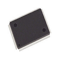
LAN91C111-NU Standard Microsystems (SMSC), LAN91C111-NU Datasheet - Page 70

LAN91C111-NU
Manufacturer Part Number
LAN91C111-NU
Description
Manufacturer
Standard Microsystems (SMSC)
Datasheet
1.LAN91C111-NU.pdf
(128 pages)
Specifications of LAN91C111-NU
Operating Supply Voltage (typ)
3.3V
Operating Supply Voltage (min)
3.135V
Operating Supply Voltage (max)
3.465V
Operating Temperature Classification
Commercial
Mounting
Surface Mount
Pin Count
128
Lead Free Status / RoHS Status
Compliant
Available stocks
Company
Part Number
Manufacturer
Quantity
Price
Company:
Part Number:
LAN91C111-NU
Manufacturer:
SMSC
Quantity:
3 000
Company:
Part Number:
LAN91C111-NU
Manufacturer:
Standard
Quantity:
12 990
Company:
Part Number:
LAN91C111-NU
Manufacturer:
SMSC
Quantity:
560
Company:
Part Number:
LAN91C111-NU
Manufacturer:
Microchip Technology
Quantity:
10 000
Part Number:
LAN91C111-NU
Manufacturer:
SMSC
Quantity:
20 000
Company:
Part Number:
LAN91C111-NU-E2
Manufacturer:
SMSC
Quantity:
415
Chapter 9 PHY MII Registers
Revision 1.91 (06-01-09)
REGISTER ADDRESS
Multiple Register Access
Multiple registers can be accessed on a single PHY Ml serial port access cycle with the multiple
register access features. The multiple register access features can be enabled by setting the multiple
register access enables bit in the PHY Ml serial port Configuration 2 register. When multiple register
access is enabled, multiple registers can be accessed on a single PHY Ml serial port access cycle by
setting the register address to 11111 during the first 16 MDC clock cycles. There is no actual register
residing in register address location 11111, so when the register address is then set to 11111, all eleven
registers are accessed on the 176 rising edges of MDC that occur after the first 16 MDC clock cycles
of the PHY Ml serial port access cycle. The registers are accessed in numerical order from 0 to 20.
After all 192 MDC clocks have been completed, all the registers have been read/written, and the serial
shift process is halted, data is latched into the device, and MDIO goes into high impedance state.
Another serial shift cycle cannot be initiated until the idle condition (at least 32 continuous 1's) is
detected.
Bit Types
Since the serial port is bi-directional, there are many types of bits. Write bits (W) are inputs during a
write cycle and are high impedance during a read cycle. Read bits (R) are outputs during a read cycle
and high impedance during a write cycle. Read/Write bits (RW) are actually write bits, which can be
read out during a read cycle. R/WSC bits are R/W bits that are self-clearing after a set period of time
or after a specific event has completed. R/LL bits are read bits that latch themselves when they go
low, and they stay latched low until read. After they are read, they are reset high. R/LH bits are the
same as R/LL bits except that they latch high. R/LT are read bits that latch themselves whenever they
make a transition or change value, and they stay latched until they are read. After R/LT bits are read,
they are updated to their current value. R/LT bits can also be programmed to assert the interrupt
function.
Bit Type Definition
R:
W:
RW:
R/LT:
6....15
2,3
16
0
1
4
5
Read Only
Write Only
Read/Write
Read/Latch on Transition
DATASHEET
70
Auto-Negotiation Remote End Capability
Auto-Negotiation Advertisement
REGISTER NAME
10/100 Non-PCI Ethernet Single Chip MAC + PHY
R/WSC:
R/LH:
R/LL:
Configuration 1
Reserved
PHY ID
Control
Status
Read/Write
Self Clearing
Read/Latch
high
Read/Latch
low
SMSC LAN91C111 REV C
Datasheet


