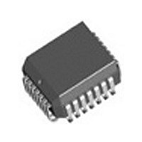
82V1671J IDT, Integrated Device Technology Inc, 82V1671J Datasheet - Page 41

82V1671J
Manufacturer Part Number
82V1671J
Description
Manufacturer
IDT, Integrated Device Technology Inc
Datasheet
1.82V1671J.pdf
(107 pages)
Specifications of 82V1671J
Number Of Channels
4
On-hook Transmission
Yes
Polarity Reversal
Yes
On-chip Ring Relay Driver
Yes
Operating Supply Voltage (typ)
3.3V
Operating Temp Range
-40C to 85C
Package Type
PLCC
Operating Temperature Classification
Industrial
Pin Count
28
Mounting
Surface Mount
Operating Current
95mA
Operating Supply Voltage (max)
3.465V
Operating Supply Voltage (min)
3.135V
Lead Free Status / RoHS Status
Not Compliant
selected to perform the measurement. The DC signal source can be
from transmit or receive path depending on the DC_SRC bit in register
LREG8:
are specified by the LM_SEL[3:0] bits in register LREG9. Refer to
- 13
filtered, A/D converted and decimated. The effective sampling rate after
the decimation stage is 8 kHz. The Offset Register here is used to
compensate for the current and voltage offset errors. See
Current Measurement” on page 45
RSLIC & CODEC CHIPSET
LM_N = 1:
LM_B = 0:
LM_B = 1:
The center frequency of the notch/bandpass filter is programmable
• DC Level Meter
If the LM_SRC bit in register LREG8 is set to 0, the DC level meter is
DC_SRC = 0: DC signal (digital) from receive path is selected;
DC_SRC = 1: DC signal from transmit path is selected.
There are a total of nine DC signal sources in the transmit path. They
As
for details.
Figure - 21
DCN-DCP
IO4-IO3
shows, the selected signal from DC transmit path is
VTAC
VDD/2
VTDC
RTIN
VCM
IO3
IO4
VL
the coefficient in the ROM is used for the notch
filter;
the coefficient in the Coe-RAM is used for the
bandpass filter;
the coefficient in the ROM is used for the
bandpass filter;
16/1
Bit LM_GF in
LREG10
Bits LM_SEL[3:0] in LREG9
MUX
Filter
Bit LM_RECT in
Rectifier
LREG10
Filter
Bit DC_OFT in LREG4
Word DC Offset in the Coe-RAM
and
2 MHz
A/D
Bits LM_EN and LM_ONCE in GREG16
Bits LM_CN[10:0] in GREG15 and GREG16
“3.9.6.7 Voltage Offset
1 MHz
A/D
VRDC
Integrator
Digital DC signal
Figure - 21 Level Meter Block Diagram
Decimation
Bits LM_TH[2:0]
Decimation
CHANNEL2
CHANNEL3
CHANNEL4
Register
CHANNEL1
in LREG10
“3.9.6.1 Offset
Offset
Table
Bits LM_FILT and LM_NOTCH in LREG8
Bits LM_B and LM_N in LREG5
LM bandpass filter coefficient
LM notch filter coefficient
Threshold
Register
Bits K[3:0] in LREG9
Notch Filter
Bandpass/
Factor
Shift
From Transmit
From Receive
41
from 300 Hz to 3400 Hz. The default center frequency is 1014 Hz. The
quality factor (Q) is fixed to 5. The filter coefficients are automatically
calculated by a software (Cal74) provided by IDT. When users input the
center frequency, this software will calculate the coefficient for the notch
or bandpass filter. By loading the coefficients to the Coe-RAM of the
CODEC, the filter characteristic can meet the requirements. Refer to
Table - 23 on page 62
Measurement” on page 49
3.9.4.2
programmable digital gain filter. The additional gain factor is either 1 or
16 depending on the LM_GF bit in register LREG10:
enough.
enabled or disabled by the LM_RECT bit in register LREG10:
The selected signal from the AC or DC path is further processed by a
LM_GF = 0:
LM_GF = 1:
The LM_GF bit should be set to 0 unless the tested signal is small
A rectifier follows to change the minus signal to plus signal. It can be
LM_RECT = 1: rectifier enabled;
LM_RECT = 0: rectifier disabled.
Bit DC_SRC in LREG8
MUX
Bits LMRH[7:0] in GREG18
Bits LMRL[7:0] in GREG17
Comparator
Register
Result
Level Meter Gain Filter and Rectifier
DC Path
AC Path
No additional gain factor;
Additional gain factor of 16.
Bit OTHRE in LREG10
Bit LM_SRC in LREG8
Bit LM_OK in LREG21
for the Coe-RAM mapping.
IDT82V1671/IDT82V1671A, IDT82V1074
MUX
for details.
Bits LM_CS[1:0]
in LREG10
MUX


