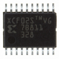
XCF02SVOG20C Xilinx Inc, XCF02SVOG20C Datasheet - Page 33

XCF02SVOG20C
Manufacturer Part Number
XCF02SVOG20C
Description
PROM, PLATFORM FLASH, 2MBIT, 20TSSOP
Manufacturer
Xilinx Inc
Datasheet
1.XCF01SVOG20C.pdf
(35 pages)
Specifications of XCF02SVOG20C
Memory Type
Flash
Memory Size
2Mbit
Clock Frequency
50MHz
Supply Voltage Range
2.3V To 2.7V, 3V To 3.6V
Memory Case Style
TSSOP
No. Of Pins
20
Operating Temperature Range
-40°C To +85°
Programmable Type
In System Programmable
Voltage - Supply
3 V ~ 3.6 V
Operating Temperature
-40°C ~ 85°C
Package / Case
20-TSSOP (0.173", 4.40mm Width)
Interface Type
Serial, Parallel, JTAG
Rohs Compliant
Yes
Lead Free Status / RoHS Status
Lead free / RoHS Compliant
Other names
122-1287-5
Available stocks
Company
Part Number
Manufacturer
Quantity
Price
Company:
Part Number:
XCF02SVOG20C
Manufacturer:
Xlinx
Quantity:
7
Company:
Part Number:
XCF02SVOG20C
Manufacturer:
XILINX
Quantity:
445
Company:
Part Number:
XCF02SVOG20C
Manufacturer:
XILINX/42
Quantity:
399
Part Number:
XCF02SVOG20C
Manufacturer:
XILINX/赛灵思
Quantity:
20 000
Company:
Part Number:
XCF02SVOG20C0936
Manufacturer:
SIPEX
Quantity:
59 427
Part Number:
XCF02SVOG20CLF
Manufacturer:
XILINX/赛灵思
Quantity:
20 000
DS123 (v2.18) May 19, 2010
Product Specification
07/20/04
10/18/04
03/14/05
07/11/05
12/29/05
Date
R
Version
2.4
2.5
2.6
2.7
2.8
• Added Pb-free package options VOG20, FSG48, and VOG48.
•
• Section
•
•
•
•
• Table
• Table
• Table
• Table
• Added Virtex-4 LX/FX/SX configuration data to Table 2.
• Corrected Virtex-II configuration data in Table 2.
• Corrected Virtex-II Pro configuration data in Table 2.
• Added Spartan®-3L configuration data to Table 2.
• Added Spartan-3E configuration data to Table 2.
• Paragraph added to FPGA Master SelectMAP (Parallel) Mode (1).
• Changes to DC Characteristics
• Changes to AC Characteristics
• Minor changes to grammar and punctuation.
• Added explanation of "Preliminary" to DC and AC Electrical Characteristics.
• Move from "Preliminary" to "Product Specification"
• Corrections to Virtex-4 configuration bitstream values
• Minor changes to
• Change to
• Change to
• Update to the first paragraph of
• Added JTAG cautionary note to
• Corrected logic values for Erase/Program (ER/PROG) Status field, IR[4], listed under
• Sections
Figure 6, page
(OPTIONAL Daisy-chained Slave FPGAs with different configurations) from DOUT to DIN.
information can be found in Package User Guide.)
Table 2, page
Table 1, page
Table 9, page
Table 10, page
• Added most parameter values for XCF08P, XCF16P, XCF32P devices.
• Added Footnote (1) to I
• Added most parameter values for XCF08P, XCF16P, XCF32P devices.
• Expanded Footnote (1) to include XCF08P, XCF16P, XCF32P devices.
• Added Footnote (8) through (11) relating to CLKOUT conditions for various parameters.
• Added rows to T
• Added rows specifying parameters with decompression for T
• Added T
• Added most parameter values for XCF08P, XCF16P, XCF32P devices.
• Separated Footnote (5) into Footnotes (5) and (6) to specify different derivations of T
• T
• I
• V
• T
• New rows added for T
page 31
Instruction Register (16 bits wide)," page
Source," page
Source," page 18
Source," page 21
depending on whether dual-purpose configuration pins persist as configuration pins, or
become general I/O pins after configuration.
I
OL
IHP.
OER
LC
CCO
"Recommended Operating Conditions," page
"DC Characteristics Over Operating Conditions," page
"AC Characteristics Over Operating Conditions," page
"AC Characteristics Over Operating Conditions When Cascading," page
changed for V
and T
"Absolute Maximum Ratings," page
changed,
added to test conditions for I
"XCFxxS and XCFxxP PROM as Configuration Slave with CLK Input Pin as Clock
"Internal Oscillator," page 8
"CLKOUT," page 8
DDC
HC
3: Removed reference to XC2VP125 FPGA.
1: Broke out V
9: Added clarification of ID code die revision bits.
16,
16, and
10: Deleted T
(setup time with decompression).
modified for 1.8V,
and
Figure 7, page
added to
"XCFxxP PROM as Configuration Master with CLK Input Pin as Clock
Page
CYC
www.xilinx.com
Platform Flash In-System Programmable Configuration PROMs
OL
"XCFxxP PROM as Configuration Master with Internal Oscillator as Clock
,
Figure 7, page
specifying parameters for parallel mode.
Page
15.
CEC
CCO
"AC Characteristics Over Operating Conditions," page
CCO
CKMIN2
and T
15.
description
specifying no-load conditions.
"IEEE 1149.1 Boundary-Scan (JTAG)," page
Page
/ V
17,
Page
OEC
CCJ
(bypass mode) and renamed T
Figure 12, page
IL
5.
17: Corrected connection name for FPGA DOUT
, I
,
description
into two separate columns.
19.
Page
ILP
Revision
5.
, I
13: Removed parameter T
IHP
18.
,and II
14: Separated V
22,
H
,
Page
Figure 13, page
16:
15:
15. Values modified for I
CLKO
CKMIN1
CCO
, T
SOL
COH
and V
23, and
from table. (T
to T
, T
5.
FF
23:
CCJ
CKMIN
, T
Figure 16,
16.
SF
parameters.
.
.
"XCFxxP
ILP
CYC
SOL
and
,
33


