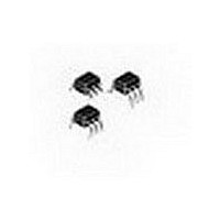
CNY171SR2M Fairchild Semiconductor, CNY171SR2M Datasheet - Page 5

CNY171SR2M
Manufacturer Part Number
CNY171SR2M
Description
Transistor Output Optocouplers Optocoupler Hi Bvceo Phototransistor
Manufacturer
Fairchild Semiconductor
Specifications of CNY171SR2M
Input Type
DC
Output Type
DC
Output Device
Transistor With Base
Number Of Elements
1
Reverse Breakdown Voltage
6V
Forward Voltage
1.65V
Forward Current
60mA
Collector-emitter Voltage
70V
Package Type
PDIP W SMD
Isolation Voltage
5250Vrms
Power Dissipation
250mW
Collector-emitter Saturation Voltage
0.4V
Current Transfer Ratio
80%
Fall Time
20000ns
Rise Time
4000ns
Pin Count
6
Mounting
Surface Mount
Operating Temp Range
-55C to 100C
Operating Temperature Classification
Industrial
Configuration
1 Channel
Maximum Collector Emitter Voltage
70 V
Maximum Collector Emitter Saturation Voltage
0.4 V
Maximum Forward Diode Voltage
1.65 V
Maximum Power Dissipation
250 mW
Maximum Operating Temperature
+ 100 C
Minimum Operating Temperature
- 55 C
Package / Case
PDIP-6 Gull Wing
Maximum Fall Time
20 us
Maximum Input Diode Current
60 mA
Maximum Reverse Diode Voltage
6 V
Maximum Rise Time
4 us
Lead Free Status / RoHS Status
Compliant
©2006 Fairchild Semiconductor Corporation
CNY17XM, CNY17FXM, MOC810XM Rev. 1.1.1
Safety and Insulation Ratings
As per IEC 60747-5-2, this optocoupler is suitable for “safe electrical insulation” only within the safety limit data.
Compliance with the safety ratings shall be ensured by means of protective circuits.
Symbol
V
V
V
RIO
CTI
IORM
IOTM
PR
Installation Classifications per DIN VDE 0110/1.89
Table 1
For Rated Main Voltage < 150Vrms
For Rated Main voltage < 300Vrms
Climatic Classification
Pollution Degree (DIN VDE 0110/1.89)
Comparative Tracking Index
Input to Output Test Voltage, Method b,
V
with tm = 1 sec, Partial Discharge < 5pC
Input to Output Test Voltage, Method a,
V
with tm = 60 sec, Partial Discharge < 5pC
Max. Working Insulation Voltage Vpeak
Highest Allowable Over Voltage Vpeak
External Creepage
External Clearance
Insulation Thickness
Insulation Resistance at Ts, V
IORM
IORM
x 1.875 = V
x 1.5 = V
PR
PR
, Type and Sample Test
Parameter
, 100% Production Test
IO
= 500V
5
Min.
1594
1275
6000
175
850
10
0.5
7
7
9
55/100/21
Typ.
I-IV
I-IV
2
Max.
www.fairchildsemi.com
V
V
V
V
Unit
mm
mm
mm
peak
peak
peak
peak


