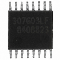
ICS307G-03LF IDT, Integrated Device Technology Inc, ICS307G-03LF Datasheet - Page 10

ICS307G-03LF
Manufacturer Part Number
ICS307G-03LF
Description
IC CLK SOURCE SRL PROGR 16-TSSOP
Manufacturer
IDT, Integrated Device Technology Inc
Type
Clock Generatorr
Specifications of ICS307G-03LF
Pll
Yes
Input
Clock, Crystal
Output
LVCMOS
Number Of Circuits
1
Ratio - Input:output
2:3
Differential - Input:output
No/No
Frequency - Max
270MHz
Divider/multiplier
Yes/No
Voltage - Supply
3 V ~ 3.6 V
Operating Temperature
0°C ~ 70°C
Mounting Type
Surface Mount
Package / Case
16-TSSOP
Frequency-max
270MHz
Number Of Elements
1
Supply Current
24mA
Pll Input Freq (min)
100KHz
Pll Input Freq (max)
300MHz
Operating Supply Voltage (typ)
3.3V
Operating Temp Range
0C to 70C
Package Type
TSSOP
Output Frequency Range
0.0002 to 270MHz
Operating Supply Voltage (min)
3V
Operating Supply Voltage (max)
3.6V
Operating Temperature Classification
Commercial
Pin Count
16
Lead Free Status / RoHS Status
Lead free / RoHS Compliant
Other names
307G-03LF
800-1028
800-1028-5
800-1028
800-1028
800-1028-5
800-1028
Available stocks
Company
Part Number
Manufacturer
Quantity
Price
Company:
Part Number:
ICS307G-03LF
Manufacturer:
IDT
Quantity:
5 985
Programming Interface
Figure 2: ICS307-03 Programming Timing Diagram
Table 8: AC Parameters for Programming the ICS307-03
Programming with VersaClock Software
The VersaClock II Software not only generates the programming word for the user, it can also be used to program the device
via the host computer’s parallel port. Demonstration boards are available from IDT that allows the VersaClock II S/W to
directly connect the ICS307-03 to a Windows based PC’s DB-25 parallel port connector and programmed simply by pressing
the “Program Part” button.
IDT® SERIALLY PROGRAMMABLE CLOCK SOURCE
ICS307-03
SERIALLY PROGRAMMABLE CLOCK SOURCE
The dynamic register within the ICS307-03 controls the entire device and may be reprogrammed any time after
power is properly applied. If V or R values are changed, the frequency will transition smoothly to the new value
without glitches or short cycles. However, changing any divider or mux in the output signal path may generate a
glitch.
The register is 132 bits in length and accepts the MSB first. The SCLK signal latches the current data bit value in
the rising edge. It latches the most recently shifted 132 bit values into the control register of device whenever CS is
high. Care must be taken to ensure that CS is always low until the system is ready to load in a new register value
and that SCLK is never toggled high when CS is high.
The register can be programmed any time after power is applied, even while in power-down (pin 15 or bit 112 held
low) with the waveform and timing shown below:.
t
DIN
CS
SCLK
setup
Parameter
t
t
SETUP
HOLD
t
t
W
S
131
130
129
t
hold
Hold time after SCLK
Strobe pulse width
SCLK Frequency
Data wait time
Setup time
Condition
128
10
2
1
Min.
2.5
2.5
2.5
10
0
t
w
Max.
200
SER PROG CLOCK SYNTHESIZER
t
s
ICS307-03
Units
MHz
ns
ns
ns
ns
REV L 032911


