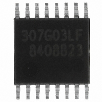
ICS307G-03LF IDT, Integrated Device Technology Inc, ICS307G-03LF Datasheet - Page 9

ICS307G-03LF
Manufacturer Part Number
ICS307G-03LF
Description
IC CLK SOURCE SRL PROGR 16-TSSOP
Manufacturer
IDT, Integrated Device Technology Inc
Type
Clock Generatorr
Specifications of ICS307G-03LF
Pll
Yes
Input
Clock, Crystal
Output
LVCMOS
Number Of Circuits
1
Ratio - Input:output
2:3
Differential - Input:output
No/No
Frequency - Max
270MHz
Divider/multiplier
Yes/No
Voltage - Supply
3 V ~ 3.6 V
Operating Temperature
0°C ~ 70°C
Mounting Type
Surface Mount
Package / Case
16-TSSOP
Frequency-max
270MHz
Number Of Elements
1
Supply Current
24mA
Pll Input Freq (min)
100KHz
Pll Input Freq (max)
300MHz
Operating Supply Voltage (typ)
3.3V
Operating Temp Range
0C to 70C
Package Type
TSSOP
Output Frequency Range
0.0002 to 270MHz
Operating Supply Voltage (min)
3V
Operating Supply Voltage (max)
3.6V
Operating Temperature Classification
Commercial
Pin Count
16
Lead Free Status / RoHS Status
Lead free / RoHS Compliant
Other names
307G-03LF
800-1028
800-1028-5
800-1028
800-1028
800-1028-5
800-1028
Available stocks
Company
Part Number
Manufacturer
Quantity
Price
Company:
Part Number:
ICS307G-03LF
Manufacturer:
IDT
Quantity:
5 985
Setting the PLL Loop Response
The PLL loop response is determined both by fixed device
characteristics and by other characterizes set by the user.
This includes the values of R
Components figure on this page.
The PLL loop bandwidth is approximated by:
The above equation calculates the “normalized” loop
bandwidth (denoted as “NBW”) which is approximately
equal to the - 3dB bandwidth. NBW does not take into
account the effects of damping factor or the second pole
imposed by C
approximation of filter performance.
Default Register Values
At power-up, the registers are set to:
ref divide = 5
VCO divide = 50
output divide = 10 (CLK1)
output divide = 2 (CLK2)
output divide = 2 (CLK3)
bit 123, 124 = 1
ICP = 3.75 µA
R = 16k
Default programming word is:
0x31FFDFFEE3BFFFFFFFFFFFFFFFF055FF2
IDT® SERIALLY PROGRAMMABLE CLOCK SOURCE
ICS307-03
SERIALLY PROGRAMMABLE CLOCK SOURCE
Where:
R
I
K
FV Divider = 12 to 2055
CP
O
S
= Value of resistor R
= VCO Gain in Hz/V
= Charge pump current in amps
NBW(PLL)
P
. It does, however, provide a useful
=
----------------------------------------- -
2
R
S
S
and C
S
FV Divider
I
in loop filter in Ohms
CP
S
as shown in the PLL
K
O
9
To prevent jitter due to modulation of the PLL by the phase
detector frequency, the following general rule should be
observed:
.
NBW(VCO PLL)
The PLL loop damping factor is determined by:
DF(VCLK)
Where:
C
S
= Value of capacitor C
= 300e
=
f(Phase Detector)
-------------------------------------- -
-12
R
----- -
2
S
in Farads
SER PROG CLOCK SYNTHESIZER
I
----------------------------------- -
10
CP
FV Divider
C
S
S
ICS307-03
in loop filter in Farads
K
O
REV L 032911


