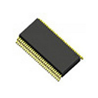
ICS932S421BGLF IDT, Integrated Device Technology Inc, ICS932S421BGLF Datasheet - Page 10

ICS932S421BGLF
Manufacturer Part Number
ICS932S421BGLF
Description
IC PCIE GEN2 MAIN CLOCK 56-TSSOP
Manufacturer
IDT, Integrated Device Technology Inc
Type
Clock Generatorr
Series
-r
Datasheet
1.ICS932S421BFLFT.pdf
(23 pages)
Specifications of ICS932S421BGLF
Frequency - Max
400MHz
Voltage - Supply
3.135 V ~ 3.465 V
Operating Temperature
0°C ~ 70°C
Mounting Type
Surface Mount
Package / Case
56-TSSOP
Frequency-max
400MHz
Number Of Elements
3
Supply Current
350mA
Pll Input Freq (min)
14.31818MHz
Operating Supply Voltage (typ)
3.3V
Operating Temp Range
0C to 70C
Package Type
TSSOP
Output Frequency Range
33.33 to 400MHz
Operating Supply Voltage (min)
3.135V
Operating Supply Voltage (max)
3.465V
Operating Temperature Classification
Commercial
Pin Count
56
Input
-
Output
-
Lead Free Status / RoHS Status
Lead free / RoHS Compliant
Output
-
Input
-
Lead Free Status / Rohs Status
Compliant
Other names
932S421BGLF
Available stocks
Company
Part Number
Manufacturer
Quantity
Price
Company:
Part Number:
ICS932S421BGLF
Manufacturer:
ICS
Quantity:
3 078
Part Number:
ICS932S421BGLFT
Manufacturer:
ICS
Quantity:
20 000
IDT
1
2
1
2
*TA = 0 - 70°C; Supply Voltage VDD = 3.3 V +/-5%
*TA = 0 - 70°C; Supply Voltage VDD = 3.3 V +/-5%
Electrical Characteristics - REF
Electrical Characteristics - Differential Jitter Parameters
Guaranteed by design and characterization, not 100% tested in production.
Guaranteed by design and characterization, not 100% tested in production.
See http://www.pcisig.com for complete specs
All Long Term Accuracy and Clock Period specifications are guaranteed assuming that REF is at 14.31818MHz
ICS932S421B
PCIe Gen2 and QPI Clock for Intel-Based Servers
TM
Absolute Clock period
Output High Voltage
Output High Current
Output Low Voltage
Output Low Current
PCIe Gen2 and QPI Clock for Intel-Based Servers
Clock High Time
Clock Low Time
Long Accuracy
PARAMETER
PARAMETER
Jitter, Phase
Clock period
Duty Cycle
Edge Rate
Rise Time
Fall Time
Skew
Jitter
t
t
SYMBOL
t
jphFBD1_3.2
jphFBD1_4.0
t
Symbol
t
jphaseHigh
t
jphasePLL
T
jphaseLo
t
t
jcyc-cyc
T
T
T
ppm
jphQPI
V
slewr/f
V
t
period
I
I
d
pabs
HIGH
t
t
LOW
sk1
OH
OL
G
G
OH
r1
f1
OL
t1
1.5MHz < f < Nyquist (50MHz)
see Tperiod min-max values
14.318MHz output including
14.318MHz output nominal
QPI 133MHz 6.4GB_12UI
V
V
Rising/Falling edge rate
OL
OH
V
V
V
10kHz < f < 1.5MHz
V
OH
CPU outputs only
OL
OL
11MHz to 33MHz
11MHz to 33MHz
= 0.4 V, V
= 2.4 V, V
OH
CONDITIONS
@MAX = 3.135 V
FBD1 3.2/4G
@ MIN = 1.95 V
I
@ MAX = 0.4 V
PCIe Gen 1
PCIe Gen 2
PCIe Gen 2
FBD1 4.8G
I
OH
V
V
V
Conditions
OL
@MIN = 1.0 V
T
T
T
1.5V
1.5V
= -1 mA
jitter
= 1.5 V
= 1.5 V
= 1.5 V
= 1 mA
OH
OL
= 2.4 V
= 0.4 V
10
27.533718
27.533718
69.8343
68.8343
MIN
-100
Min
2.4
-33
0.5
0.5
30
45
1
69.84128
TYP
TYP
0.25
1.7
2.2
2.5
40
0
2
69.8483
70.8483
MAX
1000
Max
100
N/A
N/A
500
0.4
-33
3.1
2.5
0.5
38
55
86
4
2
2
3
3
ps (p-p)
UNITS
(RMS)
(RMS)
(RMS)
(RMS)
(RMS)
Units
V/ns
ppm
mA
mA
mA
mA
ns
ns
ns
ns
ns
ns
ps
ps
ps
ps
ps
ps
ps
%
V
V
Notes
Notes
1340G—01/26/10
1,2
1,2
1,2
1,2
1,2
1,2
1,2
2
2
1
1
1
1
1
1
1
1
1
1
1
1
1
1


