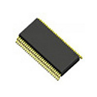
ICS932S421BGLF IDT, Integrated Device Technology Inc, ICS932S421BGLF Datasheet - Page 6

ICS932S421BGLF
Manufacturer Part Number
ICS932S421BGLF
Description
IC PCIE GEN2 MAIN CLOCK 56-TSSOP
Manufacturer
IDT, Integrated Device Technology Inc
Type
Clock Generatorr
Series
-r
Datasheet
1.ICS932S421BFLFT.pdf
(23 pages)
Specifications of ICS932S421BGLF
Frequency - Max
400MHz
Voltage - Supply
3.135 V ~ 3.465 V
Operating Temperature
0°C ~ 70°C
Mounting Type
Surface Mount
Package / Case
56-TSSOP
Frequency-max
400MHz
Number Of Elements
3
Supply Current
350mA
Pll Input Freq (min)
14.31818MHz
Operating Supply Voltage (typ)
3.3V
Operating Temp Range
0C to 70C
Package Type
TSSOP
Output Frequency Range
33.33 to 400MHz
Operating Supply Voltage (min)
3.135V
Operating Supply Voltage (max)
3.465V
Operating Temperature Classification
Commercial
Pin Count
56
Input
-
Output
-
Lead Free Status / RoHS Status
Lead free / RoHS Compliant
Output
-
Input
-
Lead Free Status / Rohs Status
Compliant
Other names
932S421BGLF
Available stocks
Company
Part Number
Manufacturer
Quantity
Price
Company:
Part Number:
ICS932S421BGLF
Manufacturer:
ICS
Quantity:
3 078
Part Number:
ICS932S421BGLFT
Manufacturer:
ICS
Quantity:
20 000
IDT
1
1
2
*TA = 0 - 70°C; Supply Voltage VDD = 3.3 V +/-5%
Absolute Maximum Rating
Electrical Characteristics - Input/Supply/Common Output Parameters
Guaranteed by design and characterization, not 100% tested in production.
Guaranteed by design and characterization, not 100% tested in production.
Input frequency should be measured at the REF pin and tuned to ideal 14.31818MHz to meet ppm frequency accuracy on PLL outputs.
Input ESD protection HBM ESD prot
3.3V Core Supply Voltage
Ambient Operating Temp
Operating Supply Current
Low-level Output Voltage
ICS932S421B
PCIe Gen2 and QPI Clock for Intel-Based Servers
3.3V Logic Input Supply
TM
Modulation Frequency
Clock/Data Rise Time
Storage Temperature
Low Threshold Input-
Low Threshold Input-
Clock/Data Fall Time
Powerdown Current
Case Temperature
Input High Voltage
Input High Current
Input Capacitance
Input Low Voltage
PCIe Gen2 and QPI Clock for Intel-Based Servers
Input Low Current
Current sinking at
Input Frequency
Clk Stabilization
Pin Inductance
SMBus Voltage
PARAMETER
PARAMETER
SCLK/SDATA
SCLK/SDATA
High Voltage
Low Voltage
V
Tdrive_PD
Trise_PD
Tfall_PD
OL
Voltage
= 0.4 V
SYMBOL
Tambient
SYMBOL
VDD_In
VDD_A
I
I
Tcase
I
V
DD3.3OP
V
DD3.3PD
T
PULLUP
C
T
T
C
V
V
V
L
C
V
I
I
IH_FS
Ts
IL_FS
STAB
I
F
RI2C
FI2C
IL1
IL2
OUT
INX
IH
pin
DD
OL
IH
IN
IL
i
V
IN
V
all differential pairs tri-stated
assertion of PD to 1st clock
From VDD Power-Up or de-
Full Active, C
IN
= 0 V; Inputs with no pull-up
CPU output enable after
Output pin capacitance
Triangular Modulation
= 0 V; Inputs with pull-up
(Min VIH + 0.15) to
(Max VIL - 0.15) to
all diff pairs driven
(Min VIH + 0.15)
PD de-assertion
(Max VIL - 0.15)
CONDITIONS*
PD rise time of
PD fall time of
CONDITIONS
X1 & X2 pins
3.3 V +/-5%
3.3 V +/-5%
3.3 V +/-5%
3.3 V +/-5%
Logic Inputs
V
V
@ I
DD
resistors
resistors
IN
= 3.3 V
PULLUP
= V
-
-
-
-
-
-
L
= Full load;
DD
6
GND - 0.5
V
V
SS
SS
2000
MIN
MIN
-200
-65
0.7
2.7
30
-5
-5
0
2
4
- 0.3
- 0.3
14.31818
TYP
TYP
V
V
V
V
DD
DD
DD
DD
MAX
MAX
1000
0.35
150
115
350
300
300
0.8
1.8
5.5
0.4
+ 0.5V
+ 0.5V
70
70
12
33
5
7
5
6
5
5
5
+ 0.3
+ 0.3
UNITS
UNITS
MHz
kHz
mA
mA
mA
mA
ms
uA
uA
uA
nH
pF
pF
pF
°
°C
°C
us
ns
ns
ns
ns
V
V
V
V
V
V
V
V
V
C
Notes
Notes
1340G—01/26/10
1
1
1
1
1
1
1
1
1
1
1
1
1
1
1
1
2
1
1
1
1
1
1
1
1
1
1
1
1
1
1


